Note
This article is a part of Arduino / ATmega328p Embedded C Firmware Programming Tutorial. Consider exploring the course home page for articles on similar topics.

Arduino Tutorial Embedded C Register Level Arduino Master Class
Also visit the Release Page for Register Level Embedded C Hardware Abstraction Library and Code for AVR.
Introduction
The Analog to Digital Converter (ADC, A/D, or A-to-D Converter) is a system that converts an analog signal (VIN) into a digital signal. The analog signal is typically a voltage that gets represented into a digital equivalent number in comparison with a reference voltage (VREF). It samples the input analog voltage and produces an output digital code for each sample measured. Analog signal can be anything ranging from microphone’s output to camera’s pixel output. For further processing of any such voltage signal, it is necessary to convert them into the digital system using ADC.
ADC converts a continuous-time and continuous-amplitude analog signal to a discrete-time and discrete-amplitude digital signal which is usually represented by 0s and 1s. The conversion involves quantization of the input, so it necessarily introduces a small amount of error or noise. Furthermore, instead of continuously performing the conversion, an ADC does the conversion periodically, sampling the input, limiting the allowable bandwidth of the input signal. There is always a loss of data when we convert an analog signal to a digital signal. We can reduce this loss by using a high resolution and high sampling rate ADC, but that increases the cost significantly. Theoretically, analog signals are continuous-time and continuous-amplitude signals thus it needs an infinite resolution and infinite sampling rate ADC to convert the analog data losslessly which is impossible to archive so the Nyquist–Shannon sampling theorem is used and the sampling rate is selected. Based on the system requirement and application it is decided which ADC will be used. Sometimes software algorithms are used to filter out quantization errors and noise.
What You Will Learn
- How does Analog to Digital Converter (ADC) work in Arduino?
- How does Analog to Digital Converter (ADC) work in AVR ATmega328p?
- What are the different types of Analog to Digital Converter (ADC)?
- What are the Properties and Specifications of Analog to Digital Converter (ADC)?
ADC Properties
Reference Voltage (VREF)
The Reference Voltage (VREF) is the standard voltage against which the analog input voltage is measured. VREF can be an input voltage provided through an external pin in the ADC or microcontroller. Some ADCs are capable of generating VREF for the ADC module using special circuitry. The range of VREF varies among different devices and the respective device datasheet must be referred to the exact value. Typically, VREF can be selected by configuring the bit field of the corresponding configuration register. The maximum voltage of analog input an ADC can convert is the VREF voltage.
Analog Input Voltage (VIN)
The Analog Input Voltage (AIN) is the voltage to be measured and converted into a digital value. The input voltage should always be less than VREF to avoid saturation of the ADC. The input voltage range is also called as conversion range.
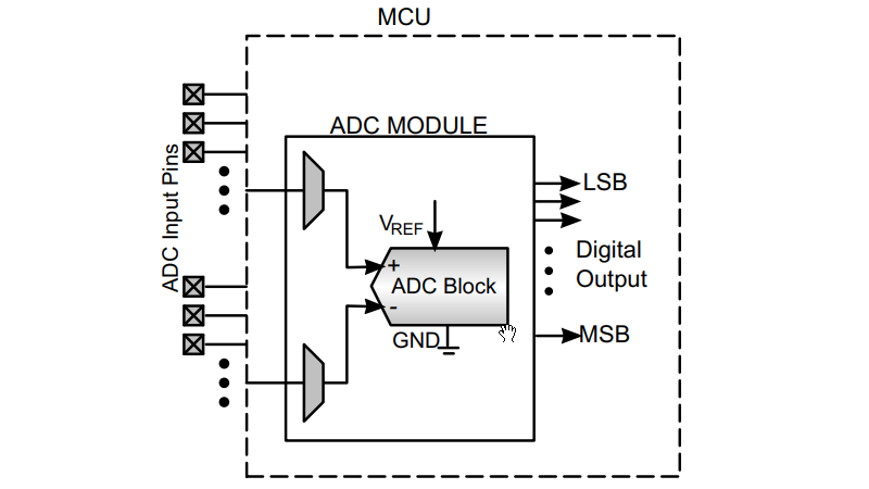
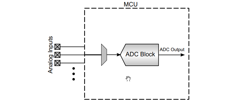
ADC modules can be classified based on the number of Analog Inputs used for a single conversion as follows:
- Single-ended Input
- Differential Input
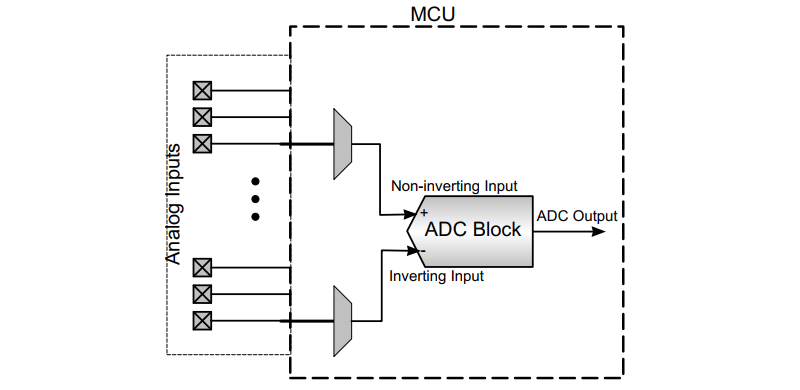
In single-ended input, the ADC sampling and conversion are performed only on one analog input signal with respect to GND and VREF.
In differential input, the difference in voltage of two analog inputs is applied to the ADC module. Differential conversions are usually operated in signed mode, where the MSB of the output code acts as the sign bit.
When using the differential mode, the offset error can be measured easily by setting up the positive and negative input on the same pin and the offset can be measured directly as the ADC does not require the ground (GND) level as a reference.
For example, when two Analog Inputs are provided, AIN1 = 2.5V & AIN2 = 0.5V, the digital value of differential output (AIN1 – AIN2 = 2V) is expected.
The ADCs whose AIN falls in the positive range 0V < AIN < VREF are called Unipolar ADC.
ADCs capable of accepting both positive and negative input voltages are called Bipolar ADC.
Resolution
The entire input voltage range (0V to VREF) is divided into a number of sub-ranges called steps. Each step is assigned a single output digital code. The number of steps is usually in powers of two (2^n). Here, n is called the Resolution of the ADC and 2^n provides the step count. For a specific VREF, the step size is determined by the resolution (VREF / 2^n). Here n also represents the number of bits in the digital output of the ADC.
For example, for an ADC with Resolution = 8 bits and VREF = 5V, the total number of steps is 256 and the step size is 19.53125mV. The output of ADC is 00000000 when VIN = 0V and output of ADC is 11111111 when VIN = 5V.
A particular resolution determines the magnitude of the quantization error and therefore determines the maximum possible signal-to-noise ratio for an ideal ADC. A step is also called LSB (least significant bit).
Quantization
Quantization is the process where the sampled analog input voltage will be replaced with an approximation from a finite set of discrete values. It is also called rounding. The LSB is determined if input analog voltage lies in the lowest step of the input voltage range.
For example, when VREF = 5V, Resolution = 8 bits, the whole range is divided into 256 steps. Analog input voltage from 0V to 19.53125mV is assigned to the same output digital code 00000000 and voltages from 20.53125mV to 39.0625mV is assigned 00000001. This process is called quantization.
There are two types of quantization:
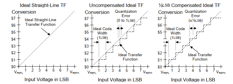
- Unadjusted / Uncompensated Quantization
The first step is taken at 1LSB, with each successive step taken at 1LSB intervals and the last step taken at VREFH – 1LSB. The quantization error (EQ) in this case is from 0LSB to 1LSB.
- Adjusted / 0.5LSB Compensated Quantization
The first step is taken at 0.5LSB, with each successive step taken at 1LSB intervals and the last step taken at VREFH – 1.5LSB. The quantization error (EQ) in this case is ±0.5LSB.
Quantization Error
Quantization error is introduced by the quantization in an ADC. It is a rounding error between the analog input voltage to the ADC and the output digitized value. The error is nonlinear and signal-dependent. As the input is a continuous-time and continuous-amplitude signal whereas the output only represents some set voltage values. All the voltage levels in between the set values are rounded off and thus introduces quantization error.
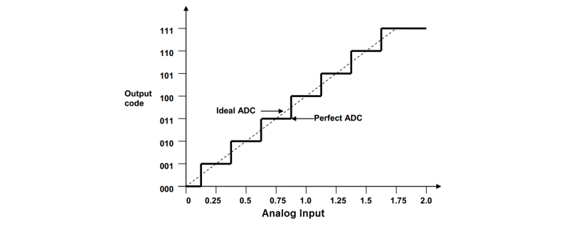
ADC Transfer Curves
Ideal ADC
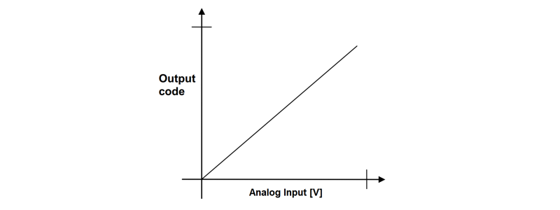
When the resolution of a specific ADC is infinite, it is called an ideal ADC. In other words, the resolution of an ideal ADC is equal to its Effective Number of Bits (ENOB). In an ideal ADC, every possible analog input value provides a unique digital output from the ADC within the specified conversion range. It is considered a theoretical concept that cannot be realized. An ideal ADC can be described mathematically using a linear transfer function.
Perfect ADC
Since ADC generates digital output, it is not possible to provide continuous output values. The perfect ADC performs the process of quantization during conversion. This results in a staircase transfer function where each step represents one LSB.
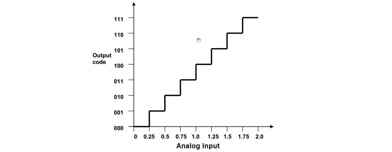
Consider an example with VREF = 2V and Resolution = 3 bit, the step size is 250mV (1 LSB). The input analog voltage ranges from 0V to 250mV will be assigned the digital output code 000 and the input analog voltage range from 251mV to 500mV will be assigned the digital code 001 and so on. The above ADC transfer graph represents this example.
This explains the quantization error due to the process of quantization. As the input voltage rises from 0V, the quantization error also rises from 0LSB and reaches a maximum quantization error of 1LSB at 250mV. Again, the quantization error increases from 0 to 1LSB as the input rises from 250mV to 500mV.
This maximum quantization error of 1LSB can be reduced to ±0.5LSB by shifting the transfer function towards the left through 0.5LSB.
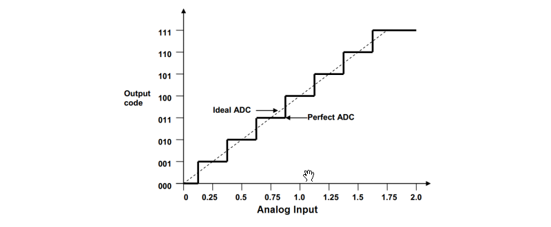
After adjusting the quantization the input voltage 0V to 0.125V is represented as 000 and from 0.126V to 0.375V is represented as 001.
ADC Properties Continues
Bandwidth
The Bandwidth represents the maximum frequency of the input analog signal that can be provided to the ADC. The bandwidth follows the Nyquist sampling theorem.
If the sampling rate of the ADC is 200kHz then the maximum frequency of analog signal the ADC can accept is 100kHz. The bandwidth of the ADC is defined as 100kHz.
While using the differential mode, the bandwidth is also limited to the frequency of the internal differential amplifier. Before providing the analog input to the ADC, any frequency component beyond the specified bandwidth must be filtered using an external filter to avoid any non-linearity.
Sampling Rate
The sampling rate is defined as the number of samples acquired in one second. The sampling rate follows the Nyquist sampling theorem. According to this theorem, the sampling rate must be at least twice the bandwidth of the input signal.
Consider the case of single ended conversion where one conversion takes 10 ADC clock cycles. Assuming the ADC clock frequency to be 1MHz, then approximately 100k samples will be converted in one second. That means the sampling rate is 100k. According to the Nyquist theorem, the maximum frequency of the analog input signal is limited to 50kHz, which represents the bandwidth of the ADC in single ended mode.
Dither
In ADCs, performance can usually be improved using dither. This is a very small amount of white noise is added to the input before conversion. Its effect is to randomize the state of the LSB based on the signal. At a lower signal voltage level, it allows the ADC to convert, at the expense of a slight increase in noise. Dithering can also increase the dynamic range of ADC.
Jitter
Jitter comes into the picture when an analog input signal has a frequency component in it. Due to the uncertainty of the ADC clock, the actual sampling time is also unpredictable. The jitter due to the ADC clock adds to the recorded noise that will reduce the effective number of bits (ENOB). The error is zero for DC, small at low frequencies, but significant with signals of high amplitude and high frequency.
Aliasing
Aliasing occurs when frequencies above the Nyquist rate are sampled which leads to incorrect frequency representation. Aliasing occurs because instantaneously sampling a function two or fewer times per cycle results in missed cycles, and therefore the appearance of an incorrectly lower frequency. For example, a 3 kHz sine wave being sampled at 2.5 kHz would be reconstructed as a 500 Hz sine wave.
To avoid aliasing, the input to an ADC must be low-pass filtered to remove frequencies above half the sampling rate. This filter is called an anti-aliasing filter and is essential for a practical ADC system that is applied to analog signals with higher frequency content. In applications where protection against aliasing is essential, oversampling may be used to greatly reduce or even eliminate it.
Oversampling
Oversampling is a process of sampling the analog input signal at a significantly higher sampling rate than the Nyquist sampling rate. The main advantages of oversampling are:
- It avoids the aliasing problem, since the sampling rate is higher compared to the Nyquist sampling rate.
- It provides a way of increasing the resolution of the ADC. For example, to implement a 14-bit converter, it is enough to have a 10-bit converter which can run at 256 times the target sampling rate. Averaging a group of 256 consecutive 10-bit samples adds four bits to the resolution of the average, producing a single sample with 14-bit resolution.
- The number of samples required to get additional n bits is = 2^2n.
- It improves the SNR of the ADC. More samples are measured to increase the resolution, which leads to reduced throughput of the ADC module. For example, a 10-bit converter with a capacity of sampling 1 kilo samples per second can be used as a 14-bit converter with a throughput of 4 samples per second.
Signal to Noise Ratio (SNR)
SNR is defined as the ratio of the output signal voltage level to the output noise level. It is usually represented in decibels (dB) and calculated using the following formula.
SNR(dB) = 20*log (Vrms of signal / Vrms of noise)
In practical applications, to achieve better performance, the SNR value of an ADC should be higher.
Signal to Noise and Distortion (SINAD)
Signal to Noise and Distortion is defined as the ratio of the RMS value of the signal amplitude to the RMS value of all other spectral components, including harmonics, but excluding DC. For representing the overall dynamic performance of an ADC, SINAD is a good choice since it includes both the noise and distortion components. It can be calculated by formula.
SINAD = (Average Power of Signal + Average Power of Noise + Average Power of Distortion) / (Average Power of Noise + Average Power of Distortion)
Effective Number Of Bits (ENOB)
The effective number of bits (ENOB) is the number of bits with which the ADC behaves like a perfect ADC. It is another way of representing the signal to noise ratio and distortion (SINAD) and can be derived from the following formula.
ENOB = (SINAD – 1.76) / 6.02
In practical applications, to achieve better performance, the ENOB value of an ADC should be as close as possible to the resolution of the ADC.
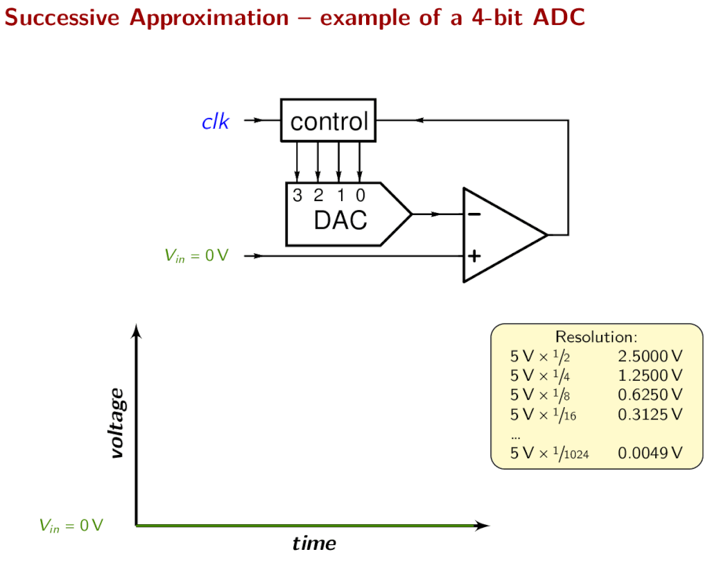
Successive Approximation ADC
Successive Approximation ADC is a type of analog to digital converter that converts a continuous analog waveform to digital data using a binary search algorithm on all possible quantization levels. The quantization level that matches the input voltage level is selected as a digital output.
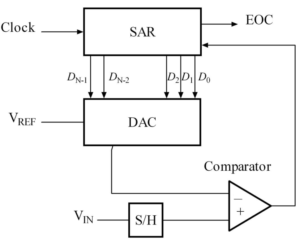
- DAC = digital-to-analog converter
- EOC = end of conversion
- SAR = successive approximation register
- S/H = sample and hold circuit
- VIN = input voltage
- VREF = reference voltage
The successive-approximation analog-to-digital converter circuit typically consists of four chief subcircuits:
- Sample and Hold Circuit
The S/H circuit is resposible to capture the input voltage (VIN) and hold it for some defined time so that the ADC can correctly do the conversion. - Comparator
The comparator is responsible to compare the VIN and DAC output. The output of comparator is given to SAR to decide if further binary search is needed. - Auccessive Approximation Register
The SAR is designed to supply an approximate digital code of VIN to the internal DAC. - Digital to Analog Converter
The DAC supplies the comparator with an analog voltage equal to the digital code output of the SAR.
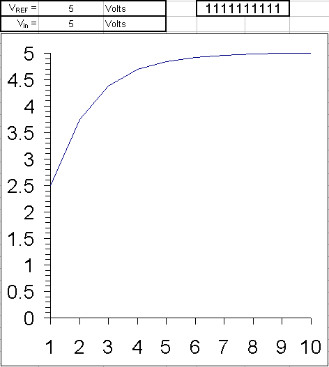
The conversion starts with initializing the most significant bit (MSB) of the SAR to 1 which is half the value of all the possible quantization levels. If the ADC is 8 bit the total quantization levels are 256 (2^8) and the SAR takes the value 127 (10000000) which is half the voltage of VREF. This value is given to the DAC to convert it into an analog voltage. The output voltage of DAC is compared with VIN by the comparator. If the DAC output exceeds the VIN then the comparator output causes the SAR to reset this MSB bit to 0 otherwise the bit is left as 1. In the next step, the next bit to MSB is set to 1 and the same process is repeated. This is the binary search algorithm.
The resulting code is the digital approximation of the sampled input voltage and is finally output by the SAR at the end of the conversion (EOC).
Applications of ADC
- Music / Audio Recording
- Digital Camera
- Signal Processing
- Sensor Interfacing

0 Comments