Note
This article is a part of Arduino / ATmega328p Embedded C Firmware Programming Tutorial. Consider exploring the course home page for articles on similar topics.

Arduino Tutorial Embedded C Register Level Arduino Master Class
Also visit the Release Page for Register Level Embedded C Hardware Abstraction Library and Code for AVR.
Introduction
This article discusses the principal clock systems in the AVR and their distribution among different hardware peripherals.
In microcontrollers, the clock rate typically refers to the frequency at which the clock generator of an MCU can generate pulses, which are used to synchronize the operations of its peripherals, and is used as an indicator of the CPU speed. It is measured in clock cycles per second or its equivalent, the SI unit hertz (Hz), but the most common microcontrollers operate in MHz. ATmega328P supports multiple clock sources which get distributed via clock multiplexer and AVR Clock Control Unit. ATmega328P can operate at a max clock rate of 20MHz.
What You Will Learn
- What are the different Clock sources are there in Arduino?
- How the CPU Clock is controlled in AVR ATmega328p chip?
- What is the CPU Clock Speed of ATmega328p?
ATmega328P Clock Distribution System
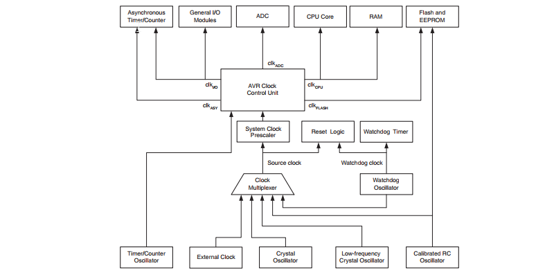
The above figure represents the clock distribution system of ATmega328P. We have three basic units Clock Sources and Input, Clock Control, Clock Output. We have multiple clock sources which get multiplexed to multiple peripherals via the AVR Clock Control Unit.
ATmega328P Clock Control Unit Outputs
- CPU Clock – clkCPU
The CPU clock is routed to parts of the system concerned with operation of the AVR Core. Examples of such modules are the General Purpose Register File, the Status Register, SRAM and the data memory holding the Stack Pointer. Halting the CPU clock inhibits the core from performing general operations and calculations.
- I/O Clock – clkI/O
The I/O clock is used by the majority of the I/O modules, like Timer/Counters, SPI, and USART. The I/O clock is also used by the External Interrupt module
- Flash Clock – clkFLASH
The Flash clock controls operation of the Flash Memory interface. The Flash clock is usually active simultaneously with the CPU clock and is responsible for memory read write.
- Asynchronous Timer Clock – clkASY
The Asynchronous Timer clock allows the Asynchronous Timer/Counter to be clocked directly from an external clock or an external 32kHz clock crystal. The dedicated clock domain allows using this Timer/Counter as an independent realtime counter even when the device is in sleep mode.
- ADC Clock – clkADC
The ADC is provided with a dedicated clock domain. This allows halting the CPU and I/O clocks while AD conversion in order to reduce noise generated by digital circuitry. This gives more accurate ADC conversion results.
ATmega328P Clock Sources
The device has the following clock source options, selectable by Flash Fuse bits as shown below. The clock from the selected source is input to the AVR clock generator and routed to the appropriate modules.
- Low Power Crystal Oscillator
- Full Swing Crystal Oscillator
- Low Frequency Crystal Oscillator
- Internal 128kHz RC Oscillator
- Calibrated Internal RC Oscillator
- External Clock
The device is shipped with an internal RC oscillator at 8.0MHz and with the fuse CKDIV8 programmed, resulting in a 1.0MHz system clock. The startup time is set to maximum and the time-out period enabled. (CKSEL = “0010”, SUT = “10”, CKDIV8 = “0”). The default setting ensures that all users can make their desired clock source setting using any available programming interface.
Low Power Crystal Oscillator
Pins XTAL1 and XTAL2 are input and output, respectively, of an inverting amplifier that can be configured for use as an On-chip Oscillator. It supports a quartz crystal or a ceramic resonator.

This Crystal Oscillator is a low power oscillator, with a reduced voltage swing on the XTAL2 output. It gives the lowest power consumption, but is not capable of driving other clock inputs, and may be more susceptible to noise in noisy environments.
If the crystal frequency exceeds the specification of the device (depends on VCC), the CKDIV8 Fuse can be programmed in order to divide the internal frequency by 8. It must be ensured that the resulting divided clock meets the frequency specification of the device.
The Low Power Oscillator can operate in three different modes, each optimized for a specific frequency range. The operating mode is selected by the fuses CKSEL3…1.
| Frequency Range (MHz) | Recommended Range for Capacitors C1 and C2 (pF) | CKSEL3…1 |
|---|---|---|
| 0.4 – 0.9 | – | 100 |
| 0.9 – 3.0 | 12 – 22 | 101 |
| 3.0 – 8.0 | 12 – 22 | 110 |
| 8.0 – 16.0 | 12 – 22 | 111 |
Full Swing Crystal Oscillator
Pins XTAL1 and XTAL2 are input and output, respectively, of an inverting amplifier that can be configured for use as an On-chip Oscillator. It supports a quartz crystal or a ceramic resonator.
This Crystal Oscillator is a full swing oscillator, with a rail-to-rail swing on the XTAL2 output. This is useful for driving other clock inputs and in noisy environments. The current consumption is higher than the ”Low Power Crystal Oscillator”. The Full Swing Crystal Oscillator will only operate for VCC = 2.7 – 5.5 volts.
If the crystal frequency exceeds the specification of the device (depends on VCC), the CKDIV8 Fuse can be programmed in order to divide the internal frequency by 8. It must be ensured that the resulting divided clock meets the frequency specification of the device.
C1 and C2 should always be equal for both crystals and resonators. The optimal value of the capacitors depends on the crystal or resonator in use, the amount of stray capacitance, and the electromagnetic noise of the environment.
| Frequency Range (MHz) | Recommended Range for Capacitors C1 and C2 (pF) | CKSEL3…1 |
|---|---|---|
| 0.4 – 20.0 | 12 – 22 | 011 |
Low Frequency Crystal Oscillator
The Low-frequency Crystal Oscillator is optimized for use with a 32.768kHz watch crystal.

The capacitance (C = Ce+Ci) needed at each TOSC pin can be calculated by using : C = 2 * CL – CS
- Ce – is optional external capacitors = C2 = C1
- Ci – is the pin capacitance
- CL – is the load capacitance for a 32.768kHz crystal
- CS – is the total stray capacitance for one TOSC pin
| Frequency Range | Start-up Time from Power-down and Power-save | CKSEL3…1 |
|---|---|---|
| 32.768kHz | 1K CK | 0100 |
| 32.768kHz | 32K CK | 0101 |
Calibrated Internal RC Oscillator
By default, the Internal RC Oscillator provides an approximate 8.0MHz clock. Though voltage and temperature dependent, this clock can be very accurately calibrated by the user. This clock may be selected as the system clock by programming the CKSEL Fuses. The device is shipped with this option selected.
If selected, it will operate with no external components. During reset, hardware loads the pre-programmed calibration value into the OSCCAL Register and thereby automatically calibrates the RC Oscillator. By changing the OSCCAL register from SW, it is possible to get a higher calibration accuracy than by using the factory calibration.
| Frequency Range (MHz) | CKSEL3…1 |
|---|---|
| 7.3 – 8.1 | 0010 |
128kHz Internal Oscillator
The 128kHz internal Oscillator is a low power Oscillator providing a clock of 128kHz. The frequency is nominal at 3V and 25 Degree C. This clock may be select as the system clock by programming the CKSEL Fuses to “11”. The 128kHz oscillator is a very low power clock source and is not designed for high accuracy.
| Frequency | CKSEL3…1 |
|---|---|
| 128kHz | 0011 |
External Clock
To drive the device from an external clock source the XTAL1 pin is connected to the clock source and the XTAL2 pin can be used as GPIO PB7.

| Frequency | CKSEL3…1 |
|---|---|
| 0 – 20MHz | 0000 |
When applying an external clock, it is required to avoid sudden changes in the applied clock frequency to ensure the stable operation of the MCU. A variation in the frequency of more than 2% from one clock cycle to the next can lead to unpredictable behavior. If changes of more than 2% are required, ensure that the MCU is kept in Reset during the changes.
Note that the System Clock Prescaler can be used to implement run-time changes of the internal clock frequency while still ensuring stable operation.
ATmega328P Clock Output Buffer
ATmega328P can output the system clock on the CLKO pin. To enable the output, the CKOUT Fuse has to be programmed. This mode is suitable when the chip clock is used to drive other circuits on the system. The clock also will be output during reset, and the normal operation of the I/O pin will be overridden when the fuse is programmed. Any clock source, including the internal RC Oscillator, can be selected when the clock is output on CLKO. If the System Clock Prescaler is used, it is the divided system clock that is output.
ATmega328P Timer/Counter Oscillator
ATmega328P uses the same crystal oscillator for Low-frequency oscillators and Timer/Counter Oscillators. ATmega328P share the Timer/Counter Oscillator Pins (TOSC1 and TOSC2) with XTAL1 and XTAL2. When using the Timer/Counter Oscillator, the system clock needs to be four times the oscillator frequency. Due to this and the pin sharing, the Timer/Counter Oscillator can only be used when the Calibrated
Internal RC Oscillator is selected as system clock source. Applying an external clock source to TOSC1 can be done if EXTCLK in the ASSR Register is written to logic one.
ATmega328P System Clock Prescaler
The ATmega328P has a system clock Prescaler, and the system clock can be divided by setting the ”CLKPR – Clock Prescale Register”. This feature can be used to decrease the system clock frequency and power consumption when the requirement for processing power is low. This can be used with all clock source options, and it will affect the clock frequency of the CPU and all synchronous peripherals. clkI/O, clkADC, clkCPU, and clkFLASH are divided by a factor.
| CLKPS3 | CLKPS2 | CLKPS1 | CLKPS0 | Clock Division Factor |
|---|---|---|---|---|
| 0 | 0 | 0 | 0 | 1 |
| 0 | 0 | 0 | 1 | 2 |
| 0 | 0 | 1 | 0 | 4 |
| 0 | 0 | 1 | 1 | 8 |
| 0 | 1 | 0 | 0 | 16 |
| 0 | 1 | 0 | 1 | 32 |
| 0 | 1 | 1 | 0 | 64 |
| 0 | 1 | 1 | 1 | 128 |
| 1 | 0 | 0 | 0 | 256 |
| 1 | 0 | 0 | 1 | Reserved |
| 1 | 0 | 1 | 0 | Reserved |
| 1 | 0 | 1 | 1 | Reserved |
| 1 | 1 | 0 | 0 | Reserved |
| 1 | 1 | 0 | 1 | Reserved |
| 1 | 1 | 1 | 0 | Reserved |
| 1 | 1 | 1 | 1 | Reserved |


1 Comment
louis katz · May 12, 2023 at 2:45 am
Thanks for this. It answered my questions enough that I could make sense of the data sheet.