Note
This article is a part of Arduino / ATmega328p Embedded C Firmware Programming Tutorial. Consider exploring the course home page for articles on similar topics.

Arduino Tutorial Embedded C Register Level Arduino Master Class
Also visit the Release Page for Register Level Embedded C Hardware Abstraction Library and Code for AVR.
Introduction
This section describes the specifics of the interrupt handling as performed in ATmega328P. It also discusses the interrupt vectors available in the chip and how they are used.
What You Will Learn
- How Iterrupts work in Arduino?
- How CPU Interrupts of AVR ATmega328p chip works?
- What are the different sources of Interrupts in ATmega328p?
- What are the difference between internal and external Interrupts in ATmega328p?
- How Interrupts are enabled or disabled in Arduino/ATmega328p?
ATmega328P Interrupt Vectors
The AVR provides several different interrupt sources. These interrupts and the separate Reset Vector each have a separate program vector in the program memory space. All interrupts are assigned individual enable bits which must be written logic one together with the Global Interrupt Enable bit in the Status Register in order to enable the interrupt.
Each Interrupt Vector occupies two instruction words inATmega328/328P. This list determines the priority levels of the different interrupts. The lower the address the higher is the priority level. The lowest addresses in the program memory space are by default defined as the Reset and Interrupt Vectors.
| Vector No. | Program Address | Source | Interrupt Definition |
|---|---|---|---|
| 1 | 0x0000 | RESET | External Pin, Power-on, Brown-out, Watchdog System Reset |
| 2 | 0x0002 | INT0 | External Interrupt Request 0 |
| 3 | 0x0004 | INT1 | External Interrupt Request 1 |
| 4 | 0x0006 | PCINT0 | Pin Change Interrupt Request 0 |
| 5 | 0x0008 | PCINT1 | Pin Change Interrupt Request 1 |
| 6 | 0x000A | PCINT2 | Pin Change Interrupt Request 2 |
| 7 | 0x000C | WDT | Watchdog Time-out Interrupt |
| 8 | 0x000E | TIMER2 COMPA | Timer/Counter2 Compare Match A |
| 9 | 0x0010 | TIMER2 COMPB | Timer/Counter2 Compare Match B |
| 10 | 0x0012 | TIMER2 OVF | Timer/Counter2 Overflow |
| 11 | 0x0014 | TIMER1 CAPT | Timer/Counter1 Capture Event |
| 12 | 0x0016 | TIMER1 COMPA | Timer/Counter1 Compare Match A |
| 13 | 0x0018 | TIMER1 COMPB | Timer/Coutner1 Compare Match B |
| 14 | 0x001A | TIMER1 OVF | Timer/Counter1 Overflow |
| 15 | 0x001C | TIMER0 COMPA | Timer/Counter0 Compare Match A |
| 16 | 0x001E | TIMER0 COMPB | Timer/Counter0 Compare Match B |
| 17 | 0x0020 | TIMER0 OVF | Timer/Counter0 Overflow |
| 18 | 0x0022 | SPI, STC | SPI Serial Transfer Complete |
| 19 | 0x0024 | USART, RX | USART Rx Complete |
| 20 | 0x0026 | USART, UDRE | USART, Data Register Empty |
| 21 | 0x0028 | USART, TX | USART, Tx Complete |
| 22 | 0x002A | ADC | ADC Conversion Complete |
| 23 | 0x002C | EE READY | EEPROM Ready |
| 24 | 0x002E | ANALOG COMP | Analog Comparator |
| 25 | 0x0030 | TWI | 2-wire Serial Interface |
| 26 | 0x0032 | SPM READY | Store Program Memory Ready |
When an interrupt occurs, the Global Interrupt Enable I-bit is cleared and all interrupts are disabled. The user software can write logic one to the I-bit to enable nested interrupts. All enabled interrupts can then interrupt the current interrupt routine. The I-bit is automatically set when a Return from Interrupt instruction – RETI – is executed. When the AVR exits from an interrupt, it will always return to the main program and execute one more instruction before any pending interrupt is served.
The interrupt execution response for all the enabled AVR interrupts is four clock cycles minimum. After four clock cycles, the program vector address for the actual interrupt handling routine is executed. During this four clock cycle period, the Program Counter is pushed onto the Stack. The vector is normally a jump to the interrupt routine, and this jump takes three clock cycles. If an interrupt occurs during the execution of a multi-cycle instruction, this instruction is completed before the interrupt is served. If an interrupt occurs when the MCU is in sleep mode, the interrupt execution response time is increased by four clock cycles. This increase comes in addition to the start-up time from the selected sleep mode.
A return from an interrupt handling routine takes four clock cycles. During these four clock cycles, the Program Counter (two bytes) is popped back from the Stack, the Stack Pointer is incremented by two, and the I-bit in SREG is set.
If the program never enables an interrupt source, the Interrupt Vectors are not used, and regular program codes can be placed at these locations. This is also the case if the Reset Vector is in the Application section while the Interrupt Vectors are in the Boot section or vice versa.
| BOOTRST | IVSEL | Reset Address | Interrupt Vectors Start Address |
|---|---|---|---|
| 1 | 0 | 0x000 | 0x002 |
| 1 | 1 | 0x000 | Boot Reset Address + 0x0002 |
| 0 | 0 | Boot Reset Address | 0x002 |
| 0 | 1 | Boot Reset Address | Boot Reset Address + 0x0002 |
MCUCR – MCU Control Register
The MCU Control Register controls the placement of the Interrupt Vector table.
| Bit | 7 | 6 | 5 | 4 | 3 | 2 | 1 | 0 |
| Read/Write Initial Value | R 0 | R/W 0 | R/W 0 | R/W 0 | R 0 | R 0 | R/W 0 | R/W 0 |
| 0x35 (0x55) | – | BODS | BODSE | PUD | – | – | IVSEL | IVCE |
- Bit 1 – IVSEL: Interrupt Vector Select
When the IVSEL bit is cleared (zero), the Interrupt Vectors are placed at the start of the Flash memory. When this bit is set (one), the Interrupt Vectors are moved to the beginning of the Boot Loader section of the Flash. - Bit 0 – IVCE: Interrupt Vector Change Enable
The IVCE bit must be written to logic one to enable change of the IVSEL bit. IVCE is cleared by hardware four cycles after it is written or when IVSEL is written.
ATmega328P External Interrupts
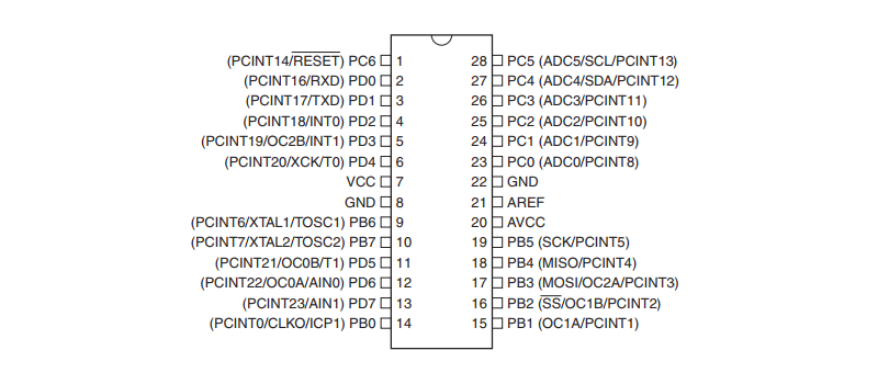
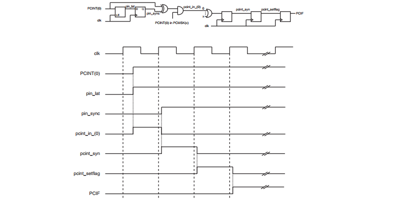
The External Interrupts are triggered by the INT0 and INT1 pins or any of the PCINT23…0 pins. The interrupts will trigger even if the INT0 and INT1 or PCINT23…0 pins are configured as outputs. This feature provides a way of generating a software interrupt. The pin change interrupt PCI2 will trigger if any enabled PCINT[23:16] pin toggles. The pin change interrupt PCI1 will trigger if any enabled PCINT[14:8] pin toggles. The pin change interrupt PCI0 will trigger if any enabled PCINT[7:0] pin toggles. The PCMSK2, PCMSK1, and PCMSK0 Registers control which pins contribute to the pin change interrupts. Pin change interrupts on PCINT23…0 are detected asynchronously. This implies that these interrupts can be used for waking the part also from sleep modes other than Idle mode.
The INT0 and INT1 interrupts can be triggered by a falling or rising edge or a low level. This is set up as indicated in the specification for the External Interrupt Control Register A – EICRA. When the INT0 or INT1 interrupts are enabled and are configured as level triggered, the interrupts will trigger as long as the pin is held low. Note that recognition of falling or rising edge interrupts on INT0 or INT1 requires the presence of an I/O clock.
EICRA – External Interrupt Control Register A
The External Interrupt Control Register A contains control bits for interrupt sense control.
| Bit | 7 | 6 | 5 | 4 | 3 | 2 | 1 | 0 |
| Read/Write Initial Value | R 0 | R 0 | R 0 | R 0 | R/W 0 | R/W 0 | R/W 0 | R/W 0 |
| 0x35 (0x55) | – | – | – | – | ISC11 | ISC10 | ISC01 | ISC00 |
- Bit 7:4 – Reserved
Unused and will always reads as zero - Bit 3, 2 – ISC11, ISC10: Interrupt Sense Control 1 Bit 1 and Bit 0
The External Interrupt 1 is activated by the external pin INT1 if the SREG I-flag and the corresponding interrupt mask are set. The value on the INT1 pin is sampled before detecting edges. If edge or toggle interrupt is selected, pulses that last longer than one clock period will generate an interrupt. Shorter pulses are not guaranteed to generate an interrupt. If low level interrupt is selected, the low level must be held until the completion of the currently executing instruction to generate an interrupt. - Bit 1, 0 – ISC01, ISC00: Interrupt Sense Control 0 Bit 1 and Bit 0
The External Interrupt 0 is activated by the external pin INT0 if the SREG I-flag and the corresponding interrupt mask are set. The value on the INT0 pin is sampled before detecting edges. If edge or toggle interrupt is selected, pulses that last longer than one clock period will generate an interrupt. Shorter pulses are not guaranteed to generate an interrupt. If low level interrupt is selected, the low level must be held until the completion of the currently executing instruction to generate an interrupt.
| ISC11 | ISC10 | Description |
|---|---|---|
| 0 | 0 | The low level of INT1 generates an interrupt request. |
| 0 | 1 | Any logical change on INT1 generates an interrupt request. |
| 1 | 0 | The falling edge of INT1 generates an interrupt request. |
| 1 | 1 | The rising edge of INT1 generates an interrupt request |
| ISC01 | ISC00 | Description |
|---|---|---|
| 0 | 0 | The low level of INT0 generates an interrupt request. |
| 0 | 1 | Any logical change on INT0 generates an interrupt request. |
| 1 | 0 | The falling edge of INT0 generates an interrupt request. |
| 1 | 1 | The rising edge of INT0 generates an interrupt request |
EIMSK – External Interrupt Mask Register
The External Interrupt Mask Register contains enables or disables the INT1 and INT0 interrupts.
| Bit | 7 | 6 | 5 | 4 | 3 | 2 | 1 | 0 |
| Read/Write Initial Value | R 0 | R 0 | R 0 | R 0 | R 0 | R 0 | R/W 0 | R/W 0 |
| 0x1D (0x3D) | – | – | – | – | – | – | INT1 | INT0 |
- Bit 7:2 – Reserved
These bits are unused bits and will always read as zero. - Bit 1 – INT1: External Interrupt Request 1 Enable
When the INT1 bit is set (one) and the I-bit in the Status Register (SREG) is set (one), the external pin interrupt is enabled. - Bit 0 – INT0: External Interrupt Request 0 Enable
When the INT0 bit is set (one) and the I-bit in the Status Register (SREG) is set (one), the external pin interrupt is enabled.
EIFR – External Interrupt Flag Register
The External Interrupt Flag Register contains the INTF1 and INTF0 flag.
| Bit | 7 | 6 | 5 | 4 | 3 | 2 | 1 | 0 |
| Read/Write Initial Value | R 0 | R 0 | R 0 | R 0 | R 0 | R 0 | R/W 0 | R/W 0 |
| 0x1C (0x3C) | – | – | – | – | – | – | INTF1 | INTF0 |
- Bit 7:2 – Reserved
These bits are unused bits and will always read as zero. - Bit 1 – INTF1: External Interrupt Flag 1
When an edge or logic change on the INT1 pin triggers an interrupt request, INTF1 becomes set (one). If the I-bit in SREG and the INT1 bit in EIMSK are set (one), the MCU will jump to the corresponding Interrupt Vector. The flag is cleared when the interrupt routine is executed. Alternatively, the flag can be cleared by writing a logical one to it. This flag is always cleared when INT1 is configured as a level interrupt. - Bit 0 – INTF0: External Interrupt Flag 0
When an edge or logic change on the INT0 pin triggers an interrupt request, INTF0 becomes set (one). If the I-bit in SREG and the INT0 bit in EIMSK are set (one), the MCU will jump to the corresponding Interrupt Vector. The flag is cleared when the interrupt routine is executed. Alternatively, the flag can be cleared by writing a logical one to it. This flag is always cleared when INT0 is configured as a level interrupt.
PCICR – Pin Change Interrupt Control Register
The Pin Change Interrupt Control Register contains enables or disables the PCI1, PCI2, PCI3.
| Bit | 7 | 6 | 5 | 4 | 3 | 2 | 1 | 0 |
| Read/Write Initial Value | R 0 | R 0 | R 0 | R 0 | R 0 | R/W 0 | R/W 0 | R/W 0 |
| (0x68) | – | – | – | – | – | PCIE2 | PCIE1 | PCIE0 |
- Bit 7:3 – Reserved
These bits are unused bits and will always read as zero. - Bit 2 – PCIE2: Pin Change Interrupt Enable 2
When the PCIE2 bit is set (one) and the I-bit in the Status Register (SREG) is set (one), pin change interrupt 2 is enabled. Any change on any enabled PCINT[23:16] pin will cause an interrupt. The corresponding interrupt of Pin Change Interrupt Request is executed from the PCI2 Interrupt Vector. PCINT[23:16] pins are enabled individually by the PCMSK2 Register. - Bit 1 – PCIE1: Pin Change Interrupt Enable 1
When the PCIE0 bit is set (one) and the I-bit in the Status Register (SREG) is set (one), pin change interrupt 0 is enabled. Any change on any enabled PCINT[7:0] pin will cause an interrupt. The corresponding interrupt of Pin Change Interrupt Request is executed from the PCI0 Interrupt Vector. PCINT[7:0] pins are enabled individually by the PCMSK0 Register.
PCIFR – Pin Change Interrupt Flag Register
The Pin Change Interrupt Flag Register contains the PCIF1, PCIF2, PCIF3 flags.
| Bit | 7 | 6 | 5 | 4 | 3 | 2 | 1 | 0 |
| Read/Write Initial Value | R 0 | R 0 | R 0 | R 0 | R 0 | R/W 0 | R/W 0 | R/W 0 |
| 0x1B (0x3B) | – | – | – | – | – | PCIE2 | PCIE1 | PCIE0 |
- Bit 7:3 – Reserved
These bits are unused bits and will always read as zero. - Bit 2 – PCIF2: Pin Change Interrupt Flag 2
When a logic change on any PCINT[23:16] pin triggers an interrupt request, PCIF2 becomes set (one). If the I-bit in SREG and the PCIE2 bit in PCICR are set (one), the MCU will jump to the corresponding Interrupt Vector. The flag is cleared when the interrupt routine is executed. Alternatively, the flag can be cleared by writing a logical one to it. - Bit 1 – PCIF1: Pin Change Interrupt Flag 1
When a logic change on any PCINT[14:8] pin triggers an interrupt request, PCIF1 becomes set (one). If the I-bit in SREG and the PCIE1 bit in PCICR are set (one), the MCU will jump to the corresponding Interrupt Vector. The flag is cleared when the interrupt routine is executed. Alternatively, the flag can be cleared by writing a logical one to it.
PCMSK2 – Pin Change Mask Register 2
| Bit | 7 | 6 | 5 | 4 | 3 | 2 | 1 | 0 |
| Read/Write Initial Value | R/W 0 | R/W 0 | R/W 0 | R/W 0 | R/W 0 | R/W 0 | R/W 0 | R/W 0 |
| (0x6D) | PCINT23 | PCINT22 | PCINT21 | PCINT20 | PCINT19 | PCINT18 | PCINT17 | PCINT16 |
- Bit 7:0 – PCINT[23:16]: Pin Change Enable Mask 23…16
Each PCINT[23:16]-bit selects whether pin change interrupt is enabled on the corresponding I/O pin. If PCINT[23:16] is set and the PCIE2 bit in PCICR is set, pin change interrupt is enabled on the corresponding I/O pin. If PCINT[23:16] is cleared, pin change interrupt on the corresponding I/O pin is disabled.
PCMSK1 – Pin Change Mask Register 1
| Bit | 7 | 6 | 5 | 4 | 3 | 2 | 1 | 0 |
| Read/Write Initial Value | R/W 0 | R/W 0 | R/W 0 | R/W 0 | R/W 0 | R/W 0 | R/W 0 | R/W 0 |
| (0x6C) | – | PCINT14 | PCINT13 | PCINT12 | PCINT11 | PCINT10 | PCINT9 | PCINT8 |
- Bit 6:0 – PCINT[14:8]: Pin Change Enable Mask 14…8
Each PCINT[14:8]-bit selects whether pin change interrupt is enabled on the corresponding I/O pin. If PCINT[14:8] is set and the PCIE1 bit in PCICR is set, pin change interrupt is enabled on the corresponding I/O pin. If PCINT[14:8] is cleared, pin change interrupt on the corresponding I/O pin is disabled.
PCMSK0 – Pin Change Mask Register 0
| Bit | 7 | 6 | 5 | 4 | 3 | 2 | 1 | 0 |
| Read/Write Initial Value | R/W 0 | R/W 0 | R/W 0 | R/W 0 | R/W 0 | R/W 0 | R/W 0 | R/W 0 |
| (0x6B) | PCINT7 | PCINT6 | PCINT5 | PCINT4 | PCINT3 | PCINT2 | PCINT1 | PCINT0 |
- Bit 6:0 – PCINT[7:0]: Pin Change Enable Mask 7…0
Each PCINT[7:0] bit selects whether pin change interrupt is enabled on the corresponding I/O pin. If PCINT[7:0] is set and the PCIE0 bit in PCICR is set, pin change interrupt is enabled on the corresponding I/O pin. If PCINT[7:0] is cleared, pin change interrupt on the corresponding I/O pin is disabled.


0 Comments