Note
This article is a part of Arduino / ATmega328p Embedded C Firmware Programming Tutorial. Consider exploring the course home page for articles on similar topics.

Arduino Tutorial Embedded C Register Level Arduino Master Class
Also visit the Release Page for Register Level Embedded C Hardware Abstraction Library and Code for AVR.
Introduction
The ATmega48A/PA/88A/PA/168A/PA/328/P features a 10-bit successive approximation ADC. The ADC is connected to an 8-channel Analog Multiplexer which allows eight single-ended voltage inputs constructed from the pins of Port A. The single-ended voltage inputs refer to 0V (GND).
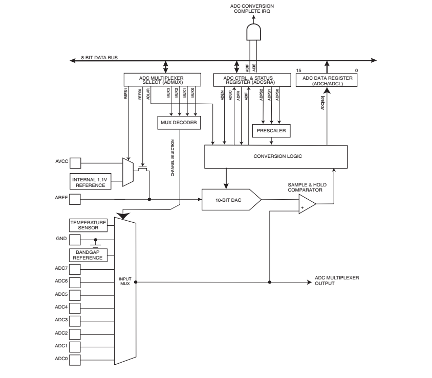
The ADC uses registers ADMUX, ADCSRA, ADCL, ADCH, ADCSRB, and DIDR0 to configure the hardware and to do analog to digital conversion. Along with register configuration, ADC hardware also needs a separate analog supply voltage pin, AVCC. AVCC must not differ more than ±0.3V from VCC. Internal reference voltages can be set at 1.1V or AVCC. When the voltage reference is selected externally the AREF pin is connected with a capacitor for better noise performance.
What You Will Learn
- What are the ADC Registers in Arduino?
- What are the ADC Registers in AVR ATmega328p?
- Which AVR Registers control and configures Analog to Digital Converter?
- What is the function of the ADC Registers?
ADMUX – ADC Multiplexer Selection Register
| Bit | 7 | 6 | 5 | 4 | 3 | 2 | 1 | 0 |
| 0x7C | REFS1 | REFS0 | ADLAR | – | MUX3 | MUX2 | MUX1 | MUX0 |
| Read/Write | R/W | R/W | R/W | R | R/W | R/W | R/W | R/W |
| Initial Value | 0 | 0 | 0 | 0 | 0 | 0 | 0 | 0 |
• Bit 7:6 – REFS[1:0]: Reference Selection Bits
These bits select the voltage reference for the ADC. The internal voltage reference options may not be used if an external reference voltage is being applied to the AREF pin.
| REFS1 | REFS0 | Voltage Reference Selection |
|---|---|---|
| 0 | 0 | AREF, Internal VREF turned off |
| 0 | 1 | AVCC with external capacitor at AREF pin |
| 1 | 0 | Reserved |
| 1 | 1 | Internal 1.1V Voltage Reference with external capacitor at AREF pin |
• Bit 5 – ADLAR: ADC Left Adjust Result
The ADLAR bit affects the presentation of the ADC conversion result in the ADC Data Register. Write one to ADLAR to left adjust the result. Otherwise, the result is right adjusted.
• Bits 3:0 – MUX[3:0]: Analog Channel Selection Bits
The value of these bits selects which analog inputs are connected to the ADC.
| MUX[3:0] | Single Ended Input |
|---|---|
| 0000 | ADC0 |
| 0001 | ADC1 |
| 0010 | ADC2 |
| 0011 | ADC3 |
| 0100 | ADC4 |
| 0101 | ADC5 |
| 0110 | ADC6 |
| 0111 | ADC7 |
| 1000 | ADC8(1) |
| 1001 | (reserved) |
| 1010 | (reserved) |
| 1011 | (reserved) |
| 1100 | (reserved) |
| 1101 | (reserved) |
| 1110 | 1.1V (VBG) |
| 1111 | 0V (GND) |
ADCSRA – ADC Control and Status Register A
| Bit | 7 | 6 | 5 | 4 | 3 | 2 | 1 | 0 |
| 0x7A | ADEN | ADSC | ADATE | ADIF | ADIE | ADPS2 | ADPS1 | ADPS0 |
| Read/Write | R/W | R/W | R/W | R/W | R/W | R/W | R/W | R/W |
| Initial Value | 0 | 0 | 0 | 0 | 0 | 0 | 0 | 0 |
• Bit 7 – ADEN: ADC Enable
Writing this bit to one enables the ADC. By writing it to zero, the ADC is turned off. Turning the ADC off while a conversion is in progress, will terminate this conversion.
• Bit 6 – ADSC: ADC Start Conversion
In Single Conversion mode, write this bit to one to start each conversion. In Free Running mode, write this bit to one that will take 25 ADC clock cycles instead of the normal 13 This first conversion performs initialization of the ADC. ADSC will read as one as long as a conversion is in progress. When the conversion is complete, it returns to zero.
• Bit 5 – ADATE: ADC Auto Trigger Enable
When this bit is written to one, Auto Triggering of the ADC is enabled. The ADC will start a conversion on a positive edge of the selected trigger signal. The trigger source is selected by setting the ADC Trigger Select bits, ADTS in
ADCSRB.
• Bit 4 – ADIF: ADC Interrupt Flag
This bit is set when an ADC conversion completes and the Data Registers are updated. The ADC Conversion Complete Interrupt is executed if the ADIE bit and the I-bit in SREG are set. ADIF is cleared by hardware when executing the corresponding interrupt handling vector.
• Bit 3 – ADIE: ADC Interrupt Enable
When this bit is written to one and the I-bit in SREG is set, the ADC Conversion Complete Interrupt is activated.
• Bits 2:0 – ADPS[2:0]: ADC Prescaler Select Bits
These bits determine the division factor between the system clock frequency and the input clock to the ADC.
| ADPS2 | ADPS1 | ADPS0 | Division Factor |
|---|---|---|---|
| 0 | 0 | 0 | 2 |
| 0 | 0 | 1 | 2 |
| 0 | 1 | 0 | 4 |
| 0 | 1 | 1 | 8 |
| 1 | 0 | 0 | 16 |
| 1 | 0 | 1 | 32 |
| 1 | 1 | 0 | 64 |
| 1 | 1 | 1 | 128 |
ADCL and ADCH – The ADC Data Register
ADLAR = 0
| Bit | 15 | 14 | 13 | 12 | 11 | 10 | 9 | 8 |
| 0x79 | – | – | – | – | – | – | ADC9 | ADC8 |
| Read/Write | R | R | R | R | R | R | R | R |
| Bit | 7 | 6 | 5 | 4 | 3 | 2 | 1 | 0 |
| 0x78 | ADC7 | ADC6 | ADC5 | ADC4 | ADC3 | ADC2 | ADC1 | ADC0 |
| Read/Write | R | R | R | R | R | R | R | R |
ADLAR = 1
| Bit | 15 | 14 | 13 | 12 | 11 | 10 | 9 | 8 |
| 0x79 | ADC9 | ADC8 | ADC7 | ADC6 | ADC5 | ADC4 | ADC3 | ADC2 |
| Read/Write | R | R | R | R | R | R | R | R |
| Bit | 7 | 6 | 5 | 4 | 3 | 2 | 1 | 0 |
| 0x78 | ADC1 | ADC0 | – | – | – | – | – | – |
| Read/Write | R | R | R | R | R | R | R | R |
When an ADC conversion is complete, the result is found in these two registers. A total of 10 bits of conversion result is stored in these two registers.
ADCSRB – ADC Control and Status Register B
| Bit | 7 | 6 | 5 | 4 | 3 | 2 | 1 | 0 |
| – | ACME | – | – | – | ADTS2 | ADTS1 | ADTS0 | |
| Read/Write | R | R/W | R | R | R | R/W | R/W | R/W |
| Initial Value | 0 | 0 | 0 | 0 | 0 | 0 | 0 | 0 |
• Bit 2:0 – ADTS[2:0]: ADC Auto Trigger Source
If ADATE in ADCSRA is written to one, the value of these bits selects which source will trigger an ADC conversion.
| ADTS2 | ADTS1 | ADTS0 | Trigger Source |
|---|---|---|---|
| 0 | 0 | 0 | Free Running mode |
| 0 | 0 | 1 | Analog Comparator |
| 0 | 1 | 0 | External Interrupt Request 0 |
| 0 | 1 | 1 | Timer/Counter0 Compare Match A |
| 1 | 0 | 0 | Timer/Counter0 Overflow |
| 1 | 0 | 1 | Timer/Counter1 Compare Match B |
| 1 | 1 | 0 | Timer/Counter1 Overflow |
| 1 | 1 | 1 | Timer/Counter1 Capture Event |
DIDR0 – Digital Input Disable Register 0
| Bit | 7 | 6 | 5 | 4 | 3 | 2 | 1 | 0 |
| 0x7E | – | – | ADC5D | ADC4D | ADC3D | ADC2D | ADC1D | ADC0D |
| Read/Write | R | R | R/W | R/W | R/W | R/W | R/W | R/W |
| Initial Value | 0 | 0 | 0 | 0 | 0 | 0 | 0 | 0 |
• Bit 5:0 – ADC5D…ADC0D: ADC5…0 Digital Input Disable
When this bit is written logic one, the digital input buffer on the corresponding ADC pin is disabled. The corresponding PIN Register bit will always read as zero when this bit is set. When an analog signal is applied to the ADC5…0 pin and the digital input from this pin is not needed, this bit should be written logic one to reduce power consumption in the digital input buffer.


2 Comments
Shriniketan · February 25, 2021 at 8:49 am
very good explanation
Crazy Engineer · March 3, 2021 at 6:20 pm
Thank You for choosing this tutorial. Keep Exploring the full series.