Note
This article is a part of Arduino / ATmega328p Embedded C Firmware Programming Tutorial. Consider exploring the course home page for articles on similar topics.

Arduino Tutorial Embedded C Register Level Arduino Master Class
Also visit the Release Page for Register Level Embedded C Hardware Abstraction Library and Code for AVR.
Introduction
In this tutorial, we will see programming techniques to program AVR GPIO as Digital Input Output. We will cover all the modes the GPIO can be programmed and we will see the practicals for each mode.
- Output – Push Pull
- Input
- Internal Pull Up
- External Pull Up
- External Pull Down
What You Will Learn
- How to Program the GPIO in Arduino?
- How to do Input Output Programming in AVR ATmega328p?
- How to control Digital Port in Arduino/ATmega328p?
- How to write Logic Data in Ports of Arduino/ATmega328p?
- How to read IO Port in Arduino/ATmega328p?
GPIO as Output – Push Pull
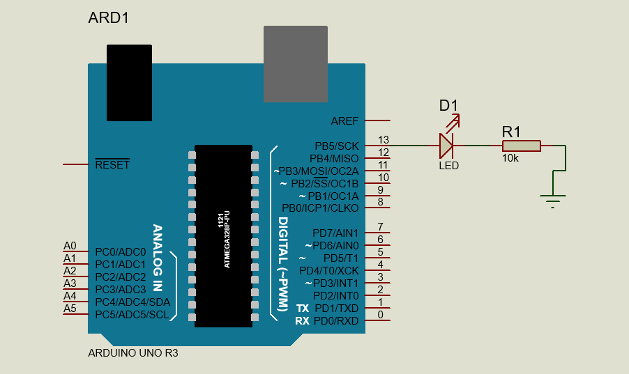
The first program of embedded systems is usually the blinky program. So let us start with the inbuilt LED in Arduino UNO. This will make things easy to start as no extra hardware is required.
The DDxn bit in the DDRx Register selects the direction of this pin. If DDxn is written logic one, Pxn is configured as an output pin. If DDxn is written logic zero, Pxn is configured as an input pin.
If PORTxn is written logic one when the pin is configured as an output pin, the port pin is driven high (one). If PORTxn is written logic zero when the pin is configured as an output pin, the port pin is driven low (zero).
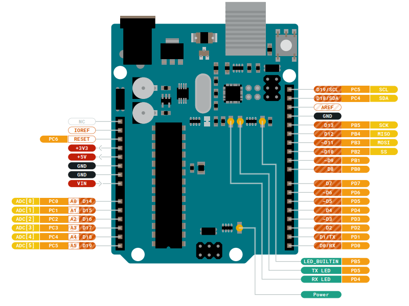
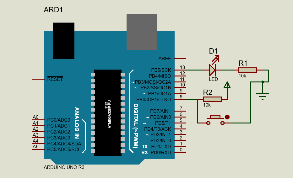
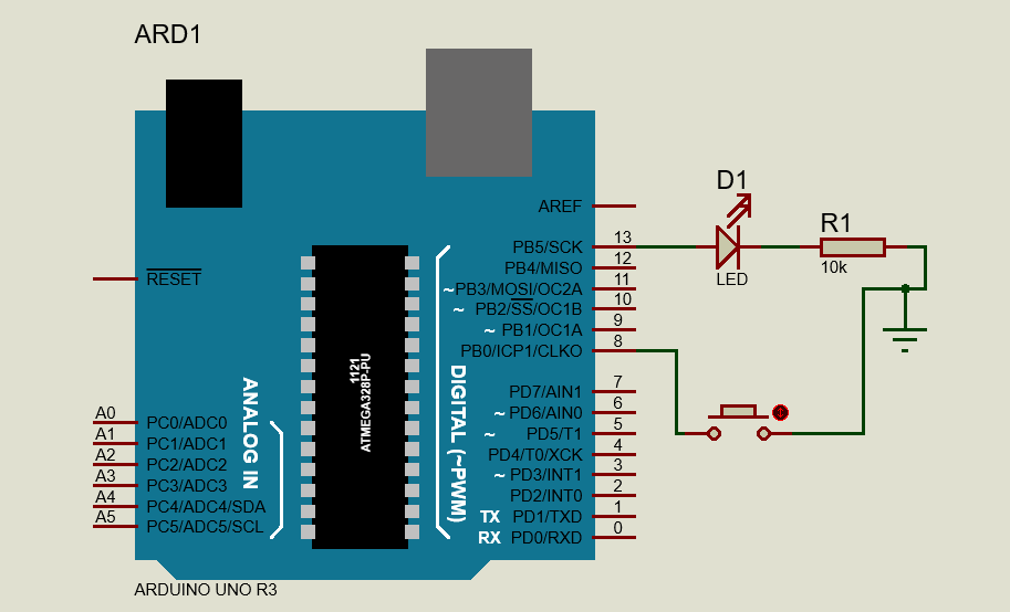
In our Arduino UNO board three (3) Ports are there in Atmega328p microcontroller : Port B [PB], Port C [PC], Port D [PD].
Port B has 8 Port Pins [PB0…PB7]. But in the Arduino UNO board, PB6 and PB7 are used for Crystal Oscillator. PB6 -> XTAL1 , PB7 -> XTAL2. So they are unusable and effectively we can use 6 Pins as GPIO.
Port C has 7 Port Pins [PC0…PC6]. But in the Arduino UNO board PC6 is used for ~RESET (Reset Pin). So effectively we can use 6 Pins as GPIO.
Port D has 8 pins [PD0…PD7]. In the
Let us look into the Schematics of Arduino UNO and see how the pins are mapped.
Programming Lab : Configuring as Output
Example 1 : Configuring all the usable pins [PB0...PB5] of Atmega328p's Port B as Output :
DDRB = 0x3F; // Using Hexadecimal Numbering System
or
DDRB = 0b0011 1111; // Using Binary Numbering System
or
*(volatile uint8_t)0x24 = 0x3F; // Address Dereferencing Method
The equivalent assembly code for any of the above lines will be :
ldi r24, 0x3F ; // Load Immediate to Register r24 [ 1 CPU Cycle ]
out 0x04, r24 ; // Store Register to I/O Location 0x04 [ 1 CPU Cycle ]
// 0x04 is DDRB's I/O address when using the I/O specific commands
IN and OUT, the I/O address when addressing I/O Registers as data space
using LD and ST instructions, 0x20 must be added. So 0x04 + 0x20 = 0x24 is
used in the 3rd method.
---------------------------------------------------------------------------
Example 2 : Configuring a single pin PB4 as Output and keeping others unchanged by bit masking :
DDRB |= 1 << 4;
or
DDRB |= 0b0001 0000;
or
DDRB |= 0x10;
The equivalent assembly code for any of the above lines will be :
sbi 0x04, 4 ; // Set Bit in I/O Register 0x04 [ 2 CPU Cycle ]
// I/O Registers within the address range 0x00 - 0x1F are directly
bit-accessible using the SBI and CBI instructions. In these registers,
the value of single bits can be checked by using the SBIS and SBIC
instructions.
---------------------------------------------------------------------------
Example 3 : Configuring multiple pins PB2, PB3, PB4 as Output with bit masking :
DDRB |= 1<<4 | 1<<3 | 1<<2;
or
DDRB |= 0b0001 1100;
or
DDRB |= 0x1C;
or
*(volatile uint8_t)0x24 |= 0x1C;
The equivalent assembly code for any of the above lines will be :
in r24, 0x04 ; // Load an I/O Location to Register r24 [ 1 CPU Cycle ]
ori r24, 0x1C ; // Logical OR r24 with Immediate value 0x1C [ 1 CPU Cycle ]
out 0x04, r24 ; // Store Register r24 to I/O Location 0x04 [ 1 CPU Cycle ]
Programming Lab : Driving the Output
Example 1 : Driving all the usable pins [PB0...PB5] of Atmega328p's Port B as HIGH : PORTB = 0x3F; // Using Hexadecimal Numbering System or PORTB = 0b0011 1111; // Using Binary Numbering System or *(volatile uint8_t)0x25 = 0x3F; // Address Dereferencing Method The equivalent assembly code for any of the above lines will be : ldi r24, 0x3F ; // Load Immediate to Register r24 [ 1 CPU Cycle ] out 0x05, r24 ; // Store Register to I/O Location 0x04 [ 1 CPU Cycle ] // 0x05 is PORTB's I/O address when using the I/O specific commands IN and OUT, the I/O address when addressing I/O Registers as data space using LD and ST instructions, 0x20 must be added. So 0x05 + 0x20 = 0x25 is used in the 3rd method. --------------------------------------------------------------------------- Example 2 : Driving a single pin PB4 as HIGH and keeping others unchanged by bit masking : PORTB |= 1 << 4; or PORTB |= 0b0001 0000; or PORTB |= 0x10; The equivalent assembly code for any of the above lines will be : sbi 0x05, 4 ; // Set Bit in I/O Register 0x05 [ 2 CPU Cycle ] // I/O Registers within the address range 0x00 - 0x1F are directly bit-accessible using the SBI and CBI instructions. In these registers, the value of single bits can be checked by using the SBIS and SBIC instructions. --------------------------------------------------------------------------- Example 3 : Driving multiple pins PB2, PB3, PB4 as HIGH with bit masking : PORTB |= 1<<4 | 1<<3 | 1<<2; or PORTB |= 0b0001 1100; or PORTB |= 0x1C; or *(volatile uint8_t)0x25 |= 0x1C; The equivalent assembly code for any of the above lines will be : in r24, 0x05 ; // Load an I/O Location to Register r24 [ 1 CPU Cycle ] ori r24, 0x1C ; // Logical OR r24 with Immediate value 0x1C [ 1 CPU Cycle ] out 0x05, r24 ; // Store Register r24 to I/O Location 0x05 [ 1 CPU Cycle ] --------------------------------------------------------------------------- Example 4 : Driving multiple pins PB1, PB2, PB5 as LOW with bit masking : PORTB &= ~(1<<5 | 1<<2 | 1<<1); or PORTB &= 0b1101 1001; or PORTB &= 0xD9; or *(volatile uint8_t)0x25 &= 0xD9; The equivalent assembly code for any of the above lines will be : in r24, 0x05 ; // Load an I/O Location to Register r24 [ 1 CPU Cycle ] andi r24, 0xD9 ; // Logical AND r24 with Immediate value 0xD9 [ 1 CPU Cycle ] out 0x05, r24 ; // Store Register r24 to I/O Location 0x05 [ 1 CPU Cycle ] --------------------------------------------------------------------------- Example 5 : Driving a single pin PB5 as LOW and keeping others unchanged by bit masking : PORTB &= ~(1 << 5); or PORTB &= 0b1101 1111; or PORTB &= 0xDF; The equivalent assembly code for any of the above lines will be : cbi 0x05, 5 ; // Clear Bit in I/O Register 0x05 [ 2 CPU Cycle ] // I/O Registers within the address range 0x00 - 0x1F are directly bit-accessible using the SBI and CBI instructions. In these registers, the value of single bits can be checked by using the SBIS and SBIC instructions.
Programming Lab : Binky LED
The onboard LED on Arduino UNO Board is connected to PB5 which is mapped to pin 13 of Arduino UNO. We will use the inbuilt <util/delay.h> for providing the delay between switching the LED on and off.
/*
 Test.c
 *
 Created: 15-09-2018 07:24:45 PM
 Author : Arnab Kumar Das
 Website : www.ArnabKumarDas.com
 */

#define F_CPU 16000000UL // Defining the CPU Frequency for Delay Calculation in delay.h
// Arduino UNO used a 16Mhz Crystal as Clock Source
#include <avr/io.h> // Contains all the I/O Register Macros
#include <avr/util.h> // Generates a Blocking Delay

 int main(void)
 {
     DDRB |= 1<<5; // Configuring PB5 as Output
     while (1)
     {
         PORTB |= 1<<5; // Writing HIGH to PB5
         _delay_ms(1000); // Delay of 1 Second
         PORTB &= ~(1<<5); // Writing LOW to PB5
         _delay_ms(1000); // Delay of 1 Second
     }
}

The equivalent assembly code will be :

sbi 0x04, 5 ;

sbi 0x05, 5 ;

ldi r18, 0xFF   ;
ldi r24, 0xD3   ;
ldi r25, 0x30   ;
subi    r18, 0x01   ;
sbci    r24, 0x00   ;
sbci    r25, 0x00   ;
brne    .-8         ;
rjmp    .+0         ;
nop

cbi 0x05, 5 ;

ldi r18, 0xFF   ;
ldi r24, 0xD3   ;
ldi r25, 0x30   ;
subi    r18, 0x01   ;
sbci    r24, 0x00   ;
sbci    r25, 0x00   ;
brne    .-8         ;
rjmp    .+0         ;
nop
rjmp    .-42        ;
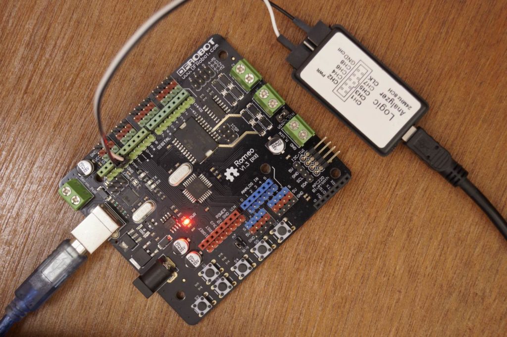
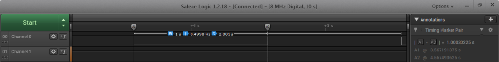
After flashing this code you should observe the onboard led to blink at every 1 second on and off delay. The above timing diagram is from the Logic Analyzer which shows an ON or OFF time of nearly 1 Second.
GPIO as Input – Internal Pull Up
If DDxn is written logic zero, Pxn is configured as an input pin.
If PORTxn is written logic one when the pin is configured as an input pin, the pull-up resistor is activated. To switch the pull-up resistor off, PORTxn has to be written logic zero, or the pin has to be configured as an output pin. The port pins are tri-stated when a
Programming Lab : Configuring as Input
Example 1 : Configuring all the usable pins [PB0...PB5] of Atmega328p's Port B as Input :
DDRB = 0xC0; // Using Hexadecimal Numbering System
or
DDRB = 0b1100 0000; // Using Binary Numbering System
or
*(volatile uint8_t)0x24 = 0xC0; // Address Dereferencing Method
The equivalent assembly code for any of the above lines will be :
ldi r24, 0xC0 ; // Load Immediate to Register r24 [ 1 CPU Cycle ]
out 0x04, r24 ; // Store Register to I/O Location 0x04 [ 1 CPU Cycle ]
// 0x04 is DDRB's I/O address when using the I/O specific commands
IN and OUT, the I/O address when addressing I/O Registers as data space
using LD and ST instructions, 0x20 must be added. So 0x04 + 0x20 = 0x24 is
used in the 3rd method.
---------------------------------------------------------------------------
Example 2 : Configuring a single pin PB4 as Input and keeping others unchanged by bit masking :
DDRB &= ~(1 << 4);
or
DDRB &= 0b1110 1111;
or
DDRB &= 0xEF;
The equivalent assembly code for any of the above lines will be :
cbi 0x04, 4 ; // Clear Bit in I/O Register 0x04 [ 2 CPU Cycle ]
// I/O Registers within the address range 0x00 - 0x1F are directly
bit-accessible using the SBI and CBI instructions. In these registers,
the value of single bits can be checked by using the SBIS and SBIC
instructions.
---------------------------------------------------------------------------
Example 3 : Configuring multiple pins PB2, PB3, PB4 as Input with bit masking :
DDRB &= ~(1<<4 | 1<<3 | 1<<2);
or
DDRB &= 0b1110 0011;
or
DDRB &= 0xE3;
or
*(volatile uint8_t)0x24 &= 0xE3;
The equivalent assembly code for any of the above lines will be :
in r24, 0x04 ; // Load an I/O Location to Register r24 [ 1 CPU Cycle ]
andi r24, 0xE3 ; // Logical AND r24 with Immediate value 0xE3 [ 1 CPU Cycle ]
out 0x04, r24 ; // Store Register r24 to I/O Location 0x04 [ 1 CPU Cycle ]
Programming Lab : Enabling the Internal Pull Up
Example 1 : Enabling Internal Pull Up on all the usable pins [PB0...PB5] of Atmega328p's Port B :

PORTB = 0xC0; // Using Hexadecimal Numbering System
or
PORTB = 0b1100 0000; // Using Binary Numbering System
or
*(volatile uint8_t)0x25 = 0xC0; // Address Dereferencing Method

The equivalent assembly code for any of the above lines will be :

ldi r24, 0xC0 ; // Load Immediate to Register r24 [ 1 CPU Cycle ]
out 0x05, r24 ; // Store Register to I/O Location 0x05 [ 1 CPU Cycle ]

---------------------------------------------------------------------------

Example 2 : Enabling Internal Pull Up on single pin PB4 with bit masking :

PORTB |= 1 << 4;
or
PORTB |= 0b0001 0000;
or
PORTB |= 0x10;

The equivalent assembly code for any of the above lines will be :

sbi 0x05, 4 ; // Set Bit in I/O Register 0x05 [ 2 CPU Cycle ]
Programming Lab : Capturing the Input
Example 1 : Capturing Input on all the usable pins [PB0...PB5] of Atmega328p's Port B :

uint8_t port_value = 0;
port_value = PINB; // Using Hexadecimal Numbering System
or
port_value = *(volatile uint8_t)0x23; // Address Dereferencing Method

Equivalent assembly code :

in r24, 0x03 ; // Store I/O Location to Register r24 [ 1 CPU Cycle ]
Programming Lab : Push Button Interfacing External Pull Up
 /*
* Test.c
*
* Created: 15-09-2018 07:24:45 PM
* Author : Arnab Kumar Das
* Website : www.ArnabKumarDas.com
*/

#define F_CPU 16000000UL // Arduino UNO use a 16Mhz Crystal as Clock Source

#include <avr/io.h> // Contains all the I/O Register Macros
#include <util/delay.h> // Generates a Blocking Delay

int main(void)
{
    DDRB |= 1 << 5; // Configuring PB5 as Output
    DDRB &= ~(1<<0); // Configuring PB0 as Input

    while (1)
    {
        if ((PINB&(1<<0)) == 1) // Reading the Pin Value
        {
            PORTB |= 1<<5; // Writing HIGH to glow LED
        }
        else
        {
            PORTB &= ~(1<<5); // Writing LOW
        }
    }
}
Programming Lab : Push Button Interfacing Internal Pull Up
/*
* Test.c
*
* Created: 15-09-2018 07:24:45 PM
* Author : Arnab Kumar Das
* Website : www.ArnabKumarDas.com
*/

#define F_CPU 16000000UL // Defining the CPU Frequency for Delay Calculation in delay.h [ Arduino UNO used a 16Mhz Crystal as Clock Source]

#include <avr/io.h> // Contains all the I/O Register Macros
#include <util/delay.h> // Generates a Blocking Delay

int main(void)
{
    DDRB |= 1 << 5; // Configuring PB5 as Output
    DDRB &= ~(1<<0); // Configuring PB0 as Input
    PORTB |= 1<<0; // Enabling Internal Pull-Up at PB0

    while (1)
    {
        if ((PINB&(1<<0)) == 1) // Reading the Pin Value
        {
            PORTB |= 1<<5; // Writing HIGH to glow LED
        }
        else
        {
            PORTB &= ~(1<<5); // Writing LOW
        }
    }
}


22 Comments
Nobel · March 1, 2023 at 6:11 pm
Hello,
I have a question about the jumps in the AVR assembly code on your webpage. Specifically, I’m confused about the behavior of the “BRNE” instruction. According to the AVR instruction set specification, the action of BRNE is “if (Z = 0) then PC = PC + k + 1”. However, in the code example on your webpage, the instruction “BRNE .-8” is used to jump to the line “SUBI r18,0x01”. Can you please clarify how this jump is made?
Thank you