Note
This article is a part of Arduino / ATmega328p Embedded C Firmware Programming Tutorial. Consider exploring the course home page for articles on similar topics.

Arduino Tutorial Embedded C Register Level Arduino Master Class
Also visit the Release Page for Register Level Embedded C Hardware Abstraction Library and Code for AVR.
Introduction
- Features
- Two Independent Output Compare Units
- Double Buffered Output Compare Registers
- Clear Timer on Compare Match (Auto Reload)
- Glitch Free, Phase Correct Pulse Width Modulator (PWM)
- Variable PWM Period
- Frequency Generator
- Three Independent Interrupt Sources (TOV0, OCF0A, and OCF0B)
Timer-0 / Counter-0 is a general purpose 8-bit Timer/Counter module, with two independent Output Compare Units, and with PWM support. It allows accurate program execution timing (event management) and wave generation.
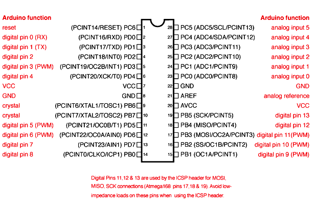
The Timer-0 has two PWM / Variable Frequency Output Pins mapped to the IO Port. OC0A is mapped to PD6 which is Digital Pin 6 on Arduino UNO board. OC0B is mapped to PD5 which is Digital Pin 5 on the Arduino UNO board.
Definations of commonly used terms in Timer
| BOTTOM | The counter reaches the BOTTOM when it becomes 0x00. |
| MAX | The counter reaches its MAXimum when it becomes 0xFF (decimal 255). |
| TOP | The counter reaches the TOP when it becomes equal to the highest value in the count sequence. The TOP value can be assigned to be the fixed value 0xFF (MAX) or the value stored in the OCR0A Register. The assignment is dependent on the mode of operation. |
What You Will Learn
- How to program the Timer-0 in Arduino?
- How to do Timer-0 Programming in AVR ATmega328p?
- What are the different modes of Timer-0 in Arduino/ATmega328p?
- What are the frequencies of counting and output in each Timer-0 modes?
Registers and Clock Source
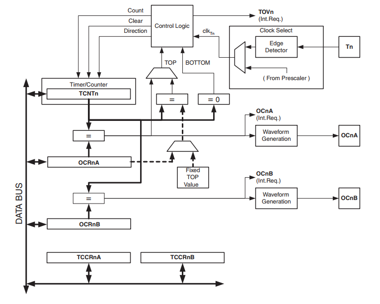
Many registers and bit references in this section are written in a general form. A lower case “n” replaces the Timer/Counter number, in this case, 0. A lower case “x” replaces the Output Compare Unit, in this case, Compare Unit A or Compare Unit B. However, when using the register or bit defines in a program, the precise form must be used, i.e., TCNT0 for accessing Timer/Counter0 counter value and so on.
The Timer/Counter can be clocked internally, via the Prescaler, or by an external clock source on the T0 pin. The Clock Select logic block controls which clock source and edge the Timer/Counter uses to increment (or decrement) its value. The Timer/Counter is inactive when no clock source is selected. The output from the Clock Select logic is referred to as the timer clock (clkT0). The clock source is selected by the Clock Select logic which is controlled by the Clock Select (CS02:0) bits located in the Timer/Counter Control Register (TCCR0B).
The double buffered Output Compare Registers (OCR0A and OCR0B) are compared with the Timer/Counter value at all times. The result of the comparison can be used by the Waveform Generator to generate a PWM or variable frequency output on the Output Compare pins (OC0A and OC0B). The compare match event will also set the Compare Flag (OCF0A or OCF0B) which can be used to generate an Output Compare interrupt request.
Counter Unit
The main part of the 8-bit Timer/Counter is the programmable bi-directional counter unit.
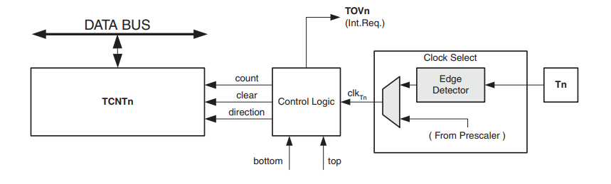
Signal Description:
| count | Increment or decrement TCNT0 by 1 |
| direction | Select between increment or decrement |
| clear | Clear TCNT0 |
| clkTn | Timer / Counter Clock |
| top | Signalize that TCNT0 has reached a maximum value |
| bottom | Signalize that TCNT0 has reached the minimum value |
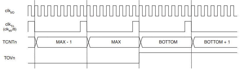
Depending on the mode of operation used, the counter is cleared, incremented, or decremented at each timer clock (clkT0). clkT0 can be generated from an external or internal clock source, selected by the Clock Select bits (CS02:0). When no clock source is selected (CS02:0 = 0) the timer is stopped. However, the TCNT0 value can be accessed by the CPU, regardless of whether clkT0 is present or not. A CPU write overrides (has priority over) all counter clear or count operations.
The counting sequence is determined by the setting of the WGM01 and WGM00 bits located in the Timer/Counter Control Register (TCCR0A) and the WGM02 bit located in the Timer/Counter Control Register B (TCCR0B). There are close connections between how the counter behaves (counts) and how waveforms are generated on the Output Compare outputs OC0A and OC0B.
The Timer/Counter Overflow Flag (TOV0) is set according to the mode of operation selected by the WGM02:0 bits. TOV0 can be used for generating a CPU interrupt.
Output Compare Unit
The 8-bit comparator continuously compares TCNT0 with the Output Compare Registers (OCR0A and OCR0B). Whenever TCNT0 equals OCR0A or OCR0B, the comparator signals a match. A match will set the Output Compare Flag (OCF0A or OCF0B) at the next timer clock cycle. If the corresponding interrupt is enabled, the Output Compare Flag generates an Output Compare interrupt. The Output Compare Flag is automatically cleared when the interrupt is executed. Alternatively, the flag can be cleared by software by writing a logical one to its I/O bit location. The Waveform Generator uses the match signal to generate an output according to operating mode set by the WGM02:0 bits and Compare Output mode (COM0x1:0) bits. The max and bottom signals are used by the Waveform Generator for handling the special cases of the extreme values in some modes of operation.
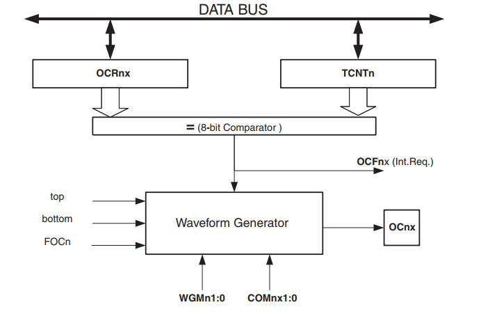
The OCR0x Registers are double buffered when using any of the Pulse Width Modulation (PWM) modes. For the normal and Clear Timer on Compare (CTC) modes of operation, the double buffering is disabled. The double buffering synchronizes the update of the OCR0x Compare Registers to either top or bottom of the counting sequence. The synchronization prevents the occurrence of odd-length, non-symmetrical PWM pulses, thereby making the output glitch-free.
The OCR0x Register access may seem complex, but this is not the case. When the double buffering is enabled, the CPU has access to the OCR0x Buffer Register, and if double buffering is disabled the CPU will access the OCR0x directly.
In non-PWM waveform generation modes, the match output of the comparator can be forced by writing a one to the Force Output Compare (FOC0x) bit. Forcing compare match will not set the OCF0x Flag or reload/clear the timer, but the OC0x pin will be updated as if a real compare match had occurred (the COM0x1:0 bits settings define whether the OC0x pin is set, cleared or toggled).
Writing TCNT0 in any mode of operation will block all compare matches for one timer clock cycle, there are risks involved when changing TCNT0 when using the Output Compare Unit, independently of whether the Timer/Counter is running or not. If the value written to TCNT0 equals the OCR0x value, the compare match will be missed, resulting in incorrect waveform generation. Similarly, do not write the TCNT0 value equal to BOTTOM when the counter is down-counting.
The setup of the OC0x should be performed before setting the Data Direction Register for the port pin to output. The easiest way of setting the OC0x value is to use the Force Output Compare (FOC0x) strobe bits in Normal mode. The OC0x Registers keep their values even when changing between Waveform Generation modes.
Compare Match Output Unit
The Compare Output mode (COM0x1:0) bits have two functions. The Waveform Generator uses the COM0x1:0 bits for defining the Output Compare (OC0x) state at the next compare match. Also, the COM0x1:0 bits control the OC0x pin output source.
The I/O Registers, I/O bits, and I/O pins in the figure are shown in bold. Only the parts of the general I/O port control registers (DDR and PORT) that are affected by the COM0x1:0 bits are shown. When referring to the OC0x state, the reference is for the internal OC0x Register, not the OC0x pin. If a system reset
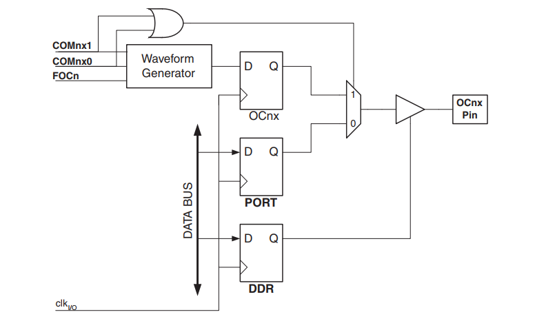
The general I/O port function is overridden by the Output Compare (OC0x) from the Waveform Generator if either of the COM0x1:0 bits is set. However, the OC0x pin direction (input or output) is still controlled by the Data Direction Register (DDR) for the port pin. The Data Direction Register bit for the OC0x pin (DDR_OC0x) must be set as an output before the OC0x value is visible on the pin. The port override function is independent of the Waveform Generation mode. The design of the Output Compare pin logic allows initialization of the OC0x state before the output is enabled.
The Waveform Generator uses the COM0x1:0 bits differently in Normal, CTC, and PWM modes. For all modes, setting the COM0x1:0 = 0 tells the Waveform Generator that no action on the OC0x Register is to be performed on the next compare match.
Modes of Operation
The mode of operation, i.e., the
Timer Normal Mode
The simplest model of operation is the Normal mode (WGM02:0 = 0). In this
Clear Timer on Compare Match (CTC) Mode
In Clear Timer on Compare or CTC mode (WGM02:0 = 2), the OCR0A Register is used to manipulate the counter resolution. In CTC mode the counter is cleared to zero when the counter value (TCNT0) matches the OCR0A. The OCR0A defines the top value for the counter, hence also its resolution. This mode allows greater control of the compare match output frequency. It also simplifies the operation of counting external events.
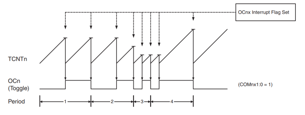
An interrupt can be generated each time the counter value reaches the TOP value by using the OCF0A Flag. If the interrupt is enabled, the interrupt handler routine can be used for updating the TOP value. However, changing TOP to a value close to BOTTOM when the counter is running with none or a low Prescaler value must be done with care since the CTC mode does not have the double buffering feature. If the new value written to OCR0A is lower than the current value of TCNT0, the counter will miss the compare match. The counter will then have to count to its maximum value (0xFF) and wrap around starting at 0x00 before the compare match can occur. For generating a waveform output in CTC mode, the OC0A output can be set to toggle its logical level on each compare match by setting the Compare Output mode bits to toggle mode (COM0A1:0 = 1). The OC0A value will not be visible on the port pin unless the data direction for the pin is set to output. The waveform generated will have a maximum frequency of fOC0 = fclk_IO/2 when OCR0A is set to zero (0x00). The waveform frequency is defined by the following equation:
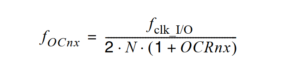
The N variable represents the prescale factor (1, 8, 64, 256, or 1024). As for the Normal mode of operation, the TOV0 Flag is set in the same timer clock cycle that the counter counts from MAX to 0x00.
Fast PWM Mode
The fast Pulse Width Modulation or fast PWM mode (WGM02:0 = 3 or 7) provides a high frequency PWM waveform generation option. The fast PWM differs from the other PWM option by its single-slope operation. The counter counts from BOTTOM to TOP then restarts from BOTTOM. TOP is defined as 0xFF when WGM2:0 = 3, and OCR0A when WGM2:0 = 7. In non-inverting Compare Output mode, the Output Compare (OC0x) is cleared on the compare match between TCNT0 and
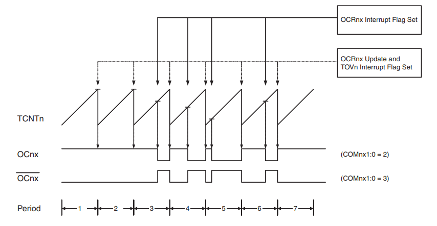
In fast PWM mode, the counter is incremented until the counter value matches the TOP value. The counter is then cleared at the following timer clock cycle. The TCNT0 value is in the timing diagram shown as a histogram for illustrating the single-slope operation. The diagram includes non-inverted and inverted PWM outputs. The small horizontal line marks on the TCNT0 slopes represent compare matches between OCR0x and TCNT0.
The Timer/Counter Overflow Flag (TOV0) is set each time the counter reaches TOP. If the interrupt is enabled, the interrupt handler routine can be used for updating the compare value. In fast PWM mode, the compare unit allows the generation of PWM waveforms on the OC0x pins. Setting the COM0x1:0 bits to two will produce a non-inverted PWM and an inverted PWM output can be generated by setting the COM0x1:0 to three: Setting the COM0A1:0 bits to one allows the OC0A pin to toggle on Compare Matches if the WGM02 bit is set. This option is not available for the OC0B pin. The actual OC0x value will only be visible on the port pin if the data direction for the port pin is set as output. The PWM waveform is generated by setting (or clearing) the OC0x Register at the compare match between OCR0x and TCNT0, and clearing (or setting) the OC0x Register at the timer clock cycle the counter is cleared (changes from TOP to BOTTOM).
The PWM frequency for the output can be calculated by the following equation :
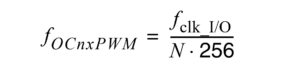
The N variable represents the prescale factor (1, 8, 64, 256, or 1024).
The extreme values for the OCR0A Register
Phase Correct PWM Mode
The phase correct PWM mode (WGM02:0 = 1 or 5) provides a high-resolution phase correct PWM waveform generation option. The phase correct PWM mode is based on a dual-slope operation. The counter counts repeatedly from BOTTOM to TOP and then from TOP to BOTTOM. TOP is defined as 0xFF when WGM2:0 = 1, and OCR0A when WGM2:0 = 5. In non-inverting Compare Output mode, the Output Compare (OC0x) is cleared on the compare match between TCNT0 and OCR0x while up-counting, and set on the compare match while down-counting. In inverting Output Compare mode, the operation is inverted. The dual-slope operation has a lower maximum operation frequency than the single-slope operation. However, due to the symmetric feature of the dual-slope PWM modes, these modes are preferred for motor control applications.
In phase correct PWM mode the counter is incremented until the counter value matches TOP. When the counter reaches TOP, it changes the count direction. The TCNT0 value will be equal to TOP for one timer clock cycle. The TCNT0 value is in the timing diagram shown as a histogram for illustrating the dual-slope operation. The diagram includes non-inverted and inverted PWM outputs. The small horizontal line marks on the TCNT0 slopes represent compare matches between OCR0x and TCNT0.
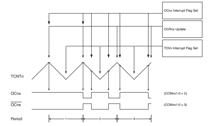
The Timer/Counter Overflow Flag (TOV0) is set each time the counter reaches BOTTOM. The Interrupt Flag can be used to generate an interrupt each time the counter reaches the BOTTOM value. In phase correct PWM mode, the compare unit allows the generation of PWM waveforms on the OC0x pins. Setting the COM0x1:0 bits to two will produce a non-inverted PWM. An inverted PWM output can be generated by setting the COM0x1:0 to three: Setting the COM0A0 bits to one allows the OC0A pin to toggle on Compare Matches if the WGM02 bit is set. This option is not available for the OC0B pin. The actual OC0x value will only be visible on the port pin if the data direction for the port pin is set as output. The PWM waveform is generated by clearing (or setting) the OC0x Register at the compare match between OCR0x and TCNT0 when the counter increments, and setting (or clearing) the OC0x Register at compare match between OCR0x and TCNT0 when the counter decrements. The PWM frequency for the output when using phase correct PWM can be calculated by the following equation:
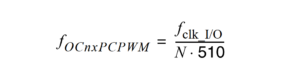
The N variable represents the prescale factor (1, 8, 64, 256, or 1024). The extreme values for the OCR0A Register represent special cases when generating a PWM waveform output in the phase correct PWM mode. If the OCR0A is set equal to BOTTOM, the output will be continuously low and if set equal to MAX the output will be continuously high for non-inverted PWM mode. For inverted PWM the output will have the opposite logic values.


4 Comments
casagoldenage · November 13, 2019 at 2:31 pm
Great article.
Crazy Engineer · November 22, 2019 at 12:58 am
Thanks for the Support. Please Like and share.
Gavin · November 16, 2019 at 9:40 am
Good article, thank you. I was trying to figure this out from the datasheet and was having issues slogging through.
Crazy Engineer · November 20, 2019 at 4:40 am
Thank You for Your Time Reading.