Note
This article is a part of Arduino / ATmega328p Embedded C Firmware Programming Tutorial. Consider exploring the course home page for articles on similar topics.

Arduino Tutorial Embedded C Register Level Arduino Master Class
Also visit the Release Page for Register Level Embedded C Hardware Abstraction Library and Code for AVR.
Introduction
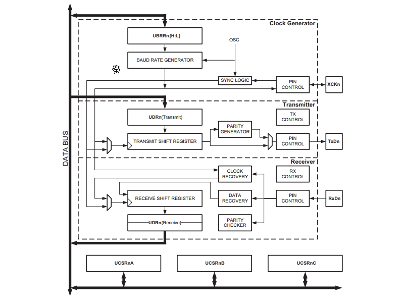
The USART (Universal Synchronous and Asynchronous Serial Receiver and Transmitter) hardware in the ATmega48A/PA/88A/PA/168A/PA/328/P microcontroller uses registers UDRn, UCSRnA, UCSRnB, UCSRnC, UBRRnL, and UBRRnH to configure the hardware and to transmit and receive data. Below are the register descriptions. The variable ‘n’ = 0 for USART0 ‘n’ = 1 for USART1 etc. The ATmega328p has only USART0.
What You Will Learn
- What are the USART/UART Registers in Arduino?
- What are the USART/UART Registers in AVR ATmega328p?
- Which AVR Registers control and configures USART/UART?
- What is the function of the AVR USART/UART Registers?
UDR0 – USART I/O Data Register
| Bit (0xC6) | 7 | 6 | 5 | 4 | 3 | 2 | 1 | 0 |
| UDR (Read) | RXB7 | RXB6 | RXB5 | RXB4 | RXB3 | RXB2 | RXB1 | RXB0 |
| UDR (Write) | TXB7 | TXB6 | TXB5 | TXB4 | TXB3 | TXB2 | TXB1 | TXB0 |
| Read/Write | R/W | R/W | R/W | R/W | R/W | R/W | R/W | R/W |
| Initial Value | 0 | 0 | 0 | 0 | 0 | 0 | 0 | 0 |
The USART Transmit Data Buffer Register and USART Receive Data Buffer Registers share the same I/O address referred to as USART Data Register or UDRn. The Transmit Data Buffer Register (TXB) will be the destination for data written to the UDRn Register location. Reading the UDR Register location will return the contents of the Receive Data Buffer Register (RXB).
When data is written to the transmit buffer, and the Transmitter is enabled, the Transmitter will load the data into the Transmit Shift Register when the Shift Register is empty. Then the data will be serially transmitted on the TxD pin.
UCSR0A – USART Control and Status Register A
| Bit | 7 | 6 | 5 | 4 | 3 | 2 | 1 | 0 |
| (0xC0) | RXC0 | TXC0 | UDRE0 | FE0 | DOR0 | UPE0 | U2X0 | MPCM0 |
| Read/Write | R | R/W | R | R | R | R | R | R |
| Initial Value | 0 | 0 | 1 | 0 | 0 | 0 | 0 | 0 |
• Bit 7 – RXC0: USART Receive Complete
This flag bit is set when there are unread data in the receive buffer and cleared when the receive buffer is empty. The RXC flag can be used to generate a receive complete interrupt.
• Bit 6 – TXC0: USART Transmit Complete
This flag bit is set when the entire frame in the transmit shift register has been shifted out and there are no new data currently present in the transmit buffer (UDR). The TXC Flag can generate a transmit complete interrupt.
• Bit 5 – UDRE0: USART Data Register Empty
The UDRE Flag indicates if the transmit buffer (UDR) is ready to receive new data. If UDRE is one, the buffer is empty, and therefore ready to be written. The UDRE Flag can generate a Data Register Empty interrupt (see description of the UDRIE bit). UDRE is set after a reset to indicate that the Transmitter is ready.
• Bit 4 – FE0: Frame Error
This bit is set if the next character in the receive buffer had a Frame Error when received. I.e., when the first stop bit of the next character in the receive buffer is zero. This bit is valid until the receive buffer (UDR) is read. The FE bit is zero when the stop bit of received data is one. Always set this bit to zero when writing to UCSRA.
• Bit 3 – DOR0: Data OverRun
This bit is set if a Data OverRun condition is detected. A Data OverRun occurs when the receive buffer is full (two characters), it is a new character waiting in the Receive Shift Register, and a new start bit is detected. This bit is valid until the receive buffer (UDR) is read. Always set this bit to zero when writing to UCSRA.
• Bit 2 – UPE0: USART Parity Error
This bit is set if the next character in the receive buffer had a Parity Error when received and the Parity Checking was enabled at that point (UPM01 = 1). This bit is valid until the receive buffer (UDR) is read. Always set this bit to zero when writing to UCSRA.
• Bit 1 – U2X0: Double the USART Transmission Speed
This bit only has an effect on the asynchronous operation. Write this bit to zero when using synchronous operation. Writing this bit to one will reduce the divisor of the baud rate divider from 16 to 8 effectively doubling the transfer rate for asynchronous communication.
• Bit 0 – MPCM0: Multi-processor Communication Mode
This bit enables the Multi-processor Communication mode. When the MPCMn bit is written to one, all the incoming frames received by the USART Receiver that do not contain address information will be ignored. The Transmitter is unaffected by the MPCM setting.
UCSR0B – USART Control and Status Register B
| Bit | 7 | 6 | 5 | 4 | 3 | 2 | 1 | 0 |
| (0xC1) | RXCIE0 | TXCIE0 | UDRIE0 | RXEN0 | TXEN0 | UCSZ02 | RXB80 | TXB80 |
| Read/Write | R/W | R/W | R/W | R/W | R/W | R/W | R | R/W |
| Initial Value | 0 | 0 | 0 | 0 | 0 | 0 | 0 | 0 |
• Bit 7 – RXCIE0: RX Complete Interrupt Enable
Writing this bit to one enables interrupt on the RXC Flag. A USART Receive Complete interrupt will be generated only if the RXCIE bit is written to one, the Global Interrupt Flag in SREG is written to one, and the RXC bit in
UCSRA is set.
• Bit 6 – TXCIE0: TX Complete Interrupt Enable
Writing this bit to one enables interrupt on the TXC Flag. A USART Transmit Complete interrupt will be generated only if the TXCIE bit is written to one, the Global Interrupt Flag in SREG is written to one and the TXC bit in UCSRA is set.
• Bit 5 – UDRIE0: USART Data Register Empty Interrupt Enable
Writing this bit to one enables interrupt on the UDRE Flag. A Data Register Empty interrupt will be generated only if the UDRIE bit is written to one, the Global Interrupt Flag in SREG is written to one and the UDRE bit in UCSRA is set.
• Bit 4 – RXEN0: Receiver Enable
Writing this bit to one enables the USART Receiver. The Receiver will override normal port operation for the RxD pin when enabled. Disabling the Receiver will flush the receive buffer invalidating the FE, DOR, and UPE Flags.
• Bit 3 – TXEN0: Transmitter Enable
Writing this bit to one enables the USART Transmitter. The Transmitter will override normal port operation for the TxD pin when enabled. The disabling of the Transmitter (writing TXEN to zero) will not become effective until ongoing and pending transmissions are completed, i.e., when the Transmit Shift Register and Transmit Buffer Register do not contain data to be transmitted. When disabled, the Transmitter will no longer override the TxD port.
• Bit 2 – UCSZ02: Character Size
The UCSZ2 bits combined with the UCSZ 1:0 bit in UCSRC sets the number of data bits (Character Size) in a frame the Receiver and Transmitter use.
• Bit 1 – RXB80: Receive Data Bit 8
RXB8 is the ninth data bit of the received character when operating with serial frames with nine data bits. Must be read before reading the low bits from UDR.
• Bit 0 – TXB80: Transmit Data Bit 8
TXB8 is the ninth data bit in the character to be transmitted when operating with serial frames with nine data bits. Must be written before writing the low bits to UDR.
UCSR0C – USART Control and Status Register C
| Bit | 7 | 6 | 5 | 4 | 3 | 2 | 1 | 0 |
| (0xC2) | UMSEL01 | UMSEL00 | UPM01 | UPM00 | USBS0 | UCSZ01 | UCSZ0 | UCPOL0 |
| Read/Write | R/W | R/W | R/W | R/W | R/W | R/W | R/W | R/W |
| Initial Value | 0 | 0 | 0 | 0 | 0 | 1 | 1 | 0 |
• Bits 7:6 – UMSEL0 1:0 USART Mode Select
These bits select the mode of operation of the USART
| UMSEL1 | UMSEL0 | Mode |
| 0 | 0 | Asynchronous USART / UART |
| 0 | 1 | Synchronous USART |
| 1 | 0 | (Reserved) |
| 1 | 1 | Master SPI (MSPIM) |
• Bits 5:4 – UPM0 1:0: Parity Mode
These bits enable and set the type of parity generation and check. If enabled, the Transmitter will automatically generate and send the parity of the transmitted data bits within each frame. The Receiver will generate a parity value for the incoming data and compare it to the UPM setting. If a mismatch is detected, the UPE Flag in UCSRA will be set.
| UPM1 | UPM0 | Parity Mode |
| 0 | 0 | Disabled |
| 0 | 1 | Reserved |
| 1 | 0 | Enabled, Even Parity |
| 1 | 1 | Enabled, Odd Parity |
• Bit 3 – USBS0: Stop Bit Select
This bit selects the number of stop bits to be inserted by the Transmitter. The Receiver ignores this setting.
| USBS | Stop Bit(s) |
| 0 | 1-bit |
| 1 | 2-bit |
• Bit 2:1 – UCSZ0 1:0: Character Size
The UCSZ 1:0 bits combined with the UCSZ 2 bit in UCSRB sets the number of data bits (Character Size) in a frame the Receiver and Transmitter use.
| UCSZ2 | UCSZ1 | UCSZ0 | Character Size |
| 0 | 0 | 0 | 5-bit |
| 0 | 0 | 1 | 6-bit |
| 0 | 1 | 0 | 7-bit |
| 0 | 1 | 1 | 8-bit |
| 1 | 0 | 0 | Reserved |
| 1 | 0 | 1 | Reserved |
| 1 | 1 | 0 | Reserved |
| 1 | 1 | 1 | 9-bit |
• Bit 0 – UCPOL0: Clock Polarity
This bit is used for synchronous mode only. Write this bit to zero when asynchronous mode is used. The UCPOL bit sets the relationship between data output change and data input sample, and the synchronous clock (XCK).
| UCPOL | Transmitted Data Changed (Output of TxD Pin) | Received Data Sampled (Input on RxD Pin) |
| 0 | Rising XCK Edge | Falling XCK Edge |
| 1 | Falling XCK Edge | Rising XCK Edge |
UBRR0L and UBRR0H – USART Baud Rate Registers
| (0xC5) | – | – | – | – | 11 | 10 | 9 | 8 |
| (0xC4) | 7 | 6 | 5 | 7 | 3 | 2 | 1 | 0 |
• Bit 15:12 – Reserved
These bits are reserved for future use. For compatibility with future devices, these bits must be written to zero when UBRRH is written.
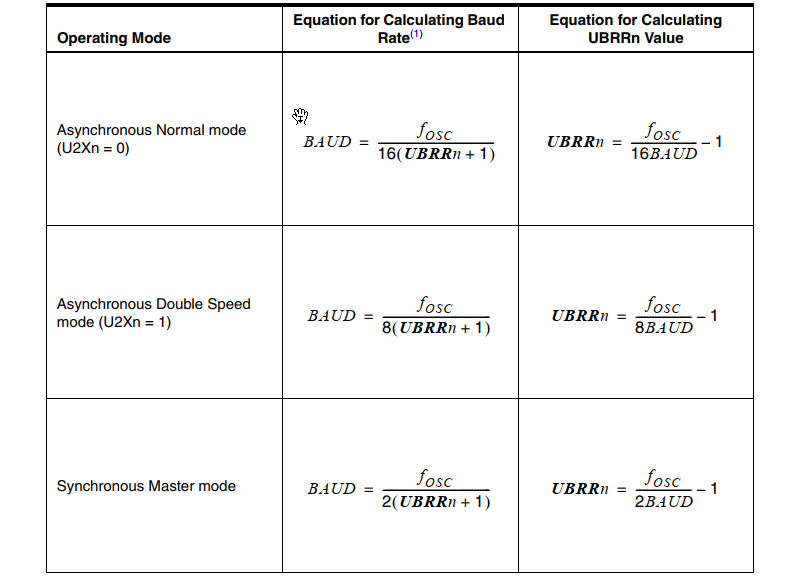
• Bit 11:0 – UBRR[11:0]: USART Baud Rate Register
This is a 12-bit register that contains the USART baud rate. The UBRRH contains the four most significant bits, and the UBRRL contains the eight least significant bits of the USART baud rate. Ongoing transmissions by the transmitter and Receiver will be corrupted if the baud rate is changed. Writing UBRRL will trigger an immediate update of the baud rate Prescaler.

0 Comments