Introduction
Once the project is conceptualised and all the components and parts are finalised it is the time to design how the components are going to work with each other and make a complete system. For a system to run properly it is important to understand what each component demand in terms of power, voltage, current, space, cooling etc. It is also important to understand the dependencies between each component. Dependencies like logic level, transmission noise, impedance etc. Please read about the previous articles about System Requirements, Component / Material selection.
A very important design aspect of this project is the PCB, as our target is to reduce the form factor of the line follower robot as much as possible which in turns reduce the weight. Small size and less weight increases efficiency and also reduces loss due to aerodynamic friction. If you see an F1 racing car you can understand how efficient it is in aerodynamics.
To improve efficiency and reduce weight, we have to remove any unnecessary component and move the Center of Mass as low as possible. To do this, I thought of using the PCB as the Chassis. This will reduce the weight and make the CM much lower, which in turn increases stability during turnings.
Making the chassis with PCB also reduces the time taken for assembly and makes things easier as we just have to solder the components at the right place and begin with testing the software. As the PCBs will be manufactured by robots and CNC machines, it looks better than any other chassis.
Software Used
For this project I have specifically using Freewares and Open Source Softwares so that Students and anyone else who don’t have access to paid softwares can also do the project efficiently and professionaly.
I used KiCad for the Schematics and PCB Design and believe me it is amazing software. Before I have used Eagle CAD and Altium but even though KiCad is free it has all the important capabilities and tools to design your PCB professionally and get it manufactured. Even it has 3D visualization available for your PCB.
The KiCad suite has five main parts:
- KiCad – the project manager.
- Eeschema – the schematic capture editor.
- Pcbnew – the PCB layout program. It also has a 3D view.
- GerbView – the Gerber viewer.
- Bitmap2Component – a tool to convert images to footprints for PCB artwork.
I am not going to show in details how to design a Schematic and PCB Layout as this is not the scope of this post/article. The main importance of this article is to showcase the output of KiCad and show how it is ordered and manufactured.
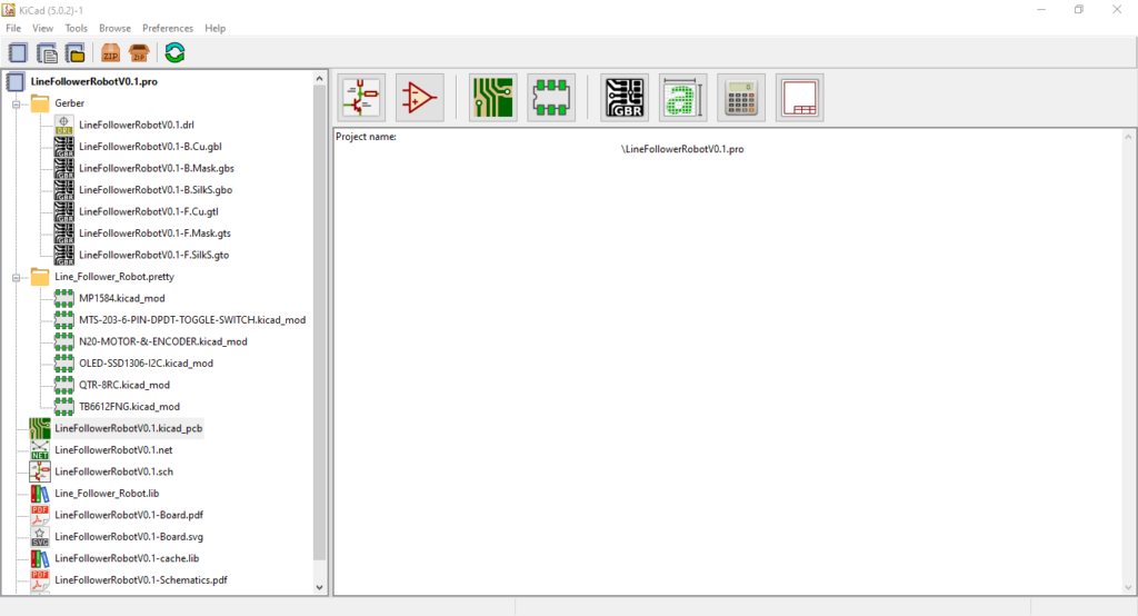
Before we begin with the Schematic design it is advisable to create a project folder and keep all files inside that. Below is an example.
Schematic
For the schematic, we have to open the Edit Schema Tool from <Tools> or Eeschema. Once open you should see an empty document in a window like below.
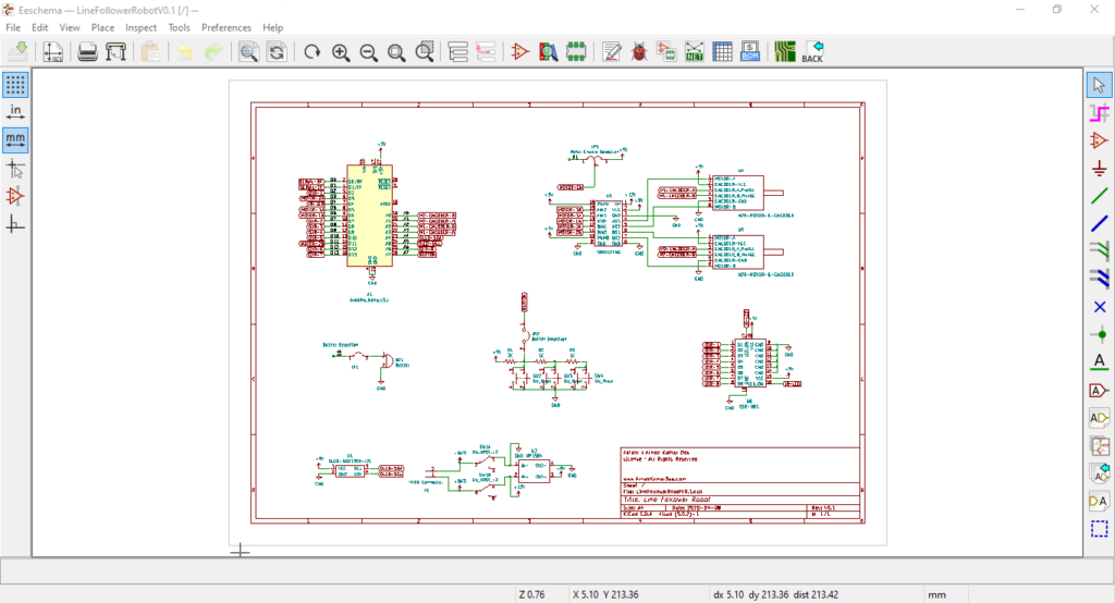
Sometimes we need to create new Schematic Symbols as the default library may not have them. You need to study the datasheet for those components and add them to a custom library as I did in my case.
I created library symbols for QTR-8RC Sensor, OLED Display SSD1306, TB6612FNG Motor Driver Board, N20 Motor with Encoders.
Once the library symbols are created I connected them together to form a system.
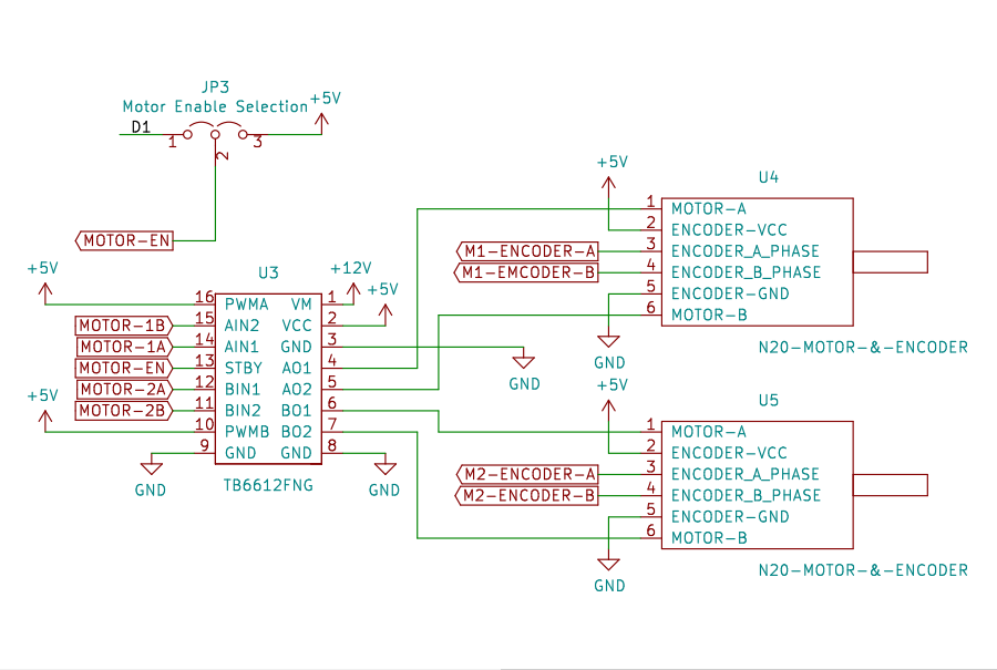
You can download the Schematic from the link below. Later at the end of the tutorial, I will add some good tutorials for KiCad for you to learn and do it by yourself.
PCB Layout
Once the Schematic is finished it is time to move to layout the PCB board. Sometimes you also need to create the footprint of some components if they are not present in the library. To create footprint you can use Footprint Library Editor Tool in KiCad.
I have used two layer design here because it makes it very easy to layout when you have many components distributed on the board.
To start with the PCB Design we have to open the PCB Layout Editor program in KiCad. You should see something like below but with an empty document in it.
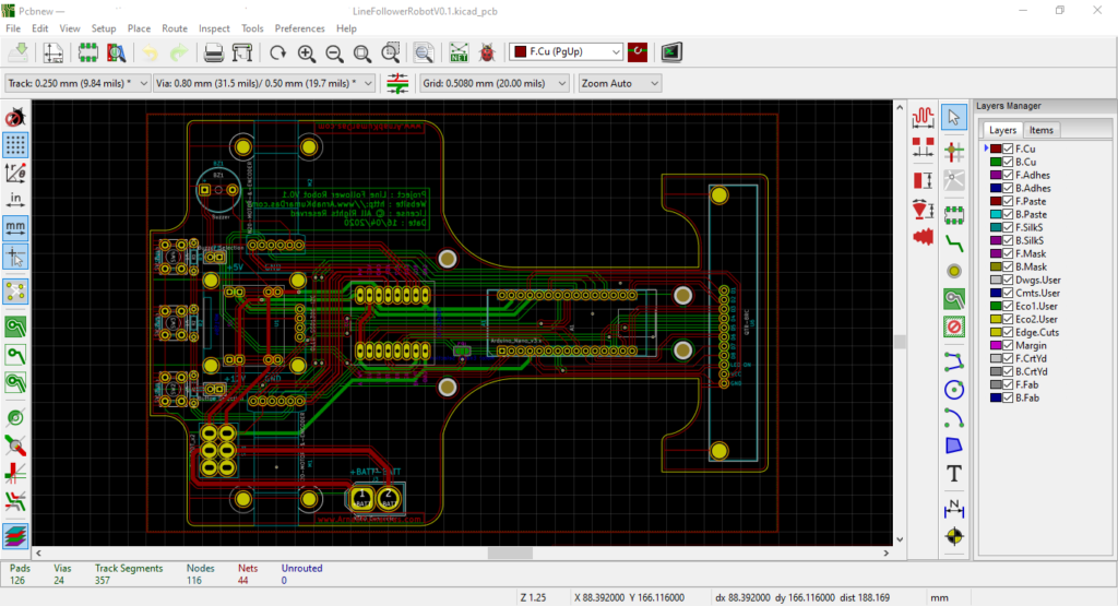
We will be Using NextPCB as the PCB Manufacturing Service so it is important to see what is the minimum and maximum technical limits they have for their manufacturing. To check that we need to visit their Capabilities Page. The main parameters that we have to check are :
| Max. Dimension | 510*590mm |
| Min. Trace | 4mil / 0.1mm |
| Min. Trace Spacing | 4mil / 0.1mm |
| Min. hole size | 0.3mm |
| Min. Via diameter | 0.45mm |
| Via To Trace Spacing | ≥5mil |
| Drill Hole Size | 0.2-6.3mm |
| Trace to Outline | ≥0.4mm |
Based on the Above Parameters we have to adjust our Design Rules in KiCad Layout Editor.
![Design Rules Used for Line Follower Robot PCB [ All in mm ]](https://www.arnabkumardas.com/blog/wp-content/uploads/2020/04/image-5.png)
At the end of the tutorial, I will attach some good tutorial about PCB Designing in KiCad that you can learn from. Below is the attached PCB Design that you can use for your reference.
PCB Manufacturing
Before we manufacture the PCB in a PCB Fabrication House / Industry like NextPCB, we need to convert our design into a manufacturable format which can be read by the machines of the industry.
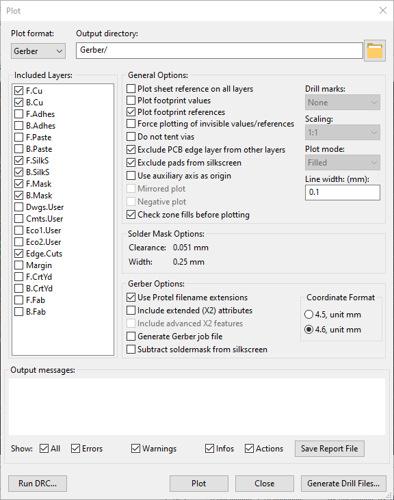
The above settings were used for the generation of all the Gerber files. it is advised that you export the files in a separate Gerber folder as I have done.
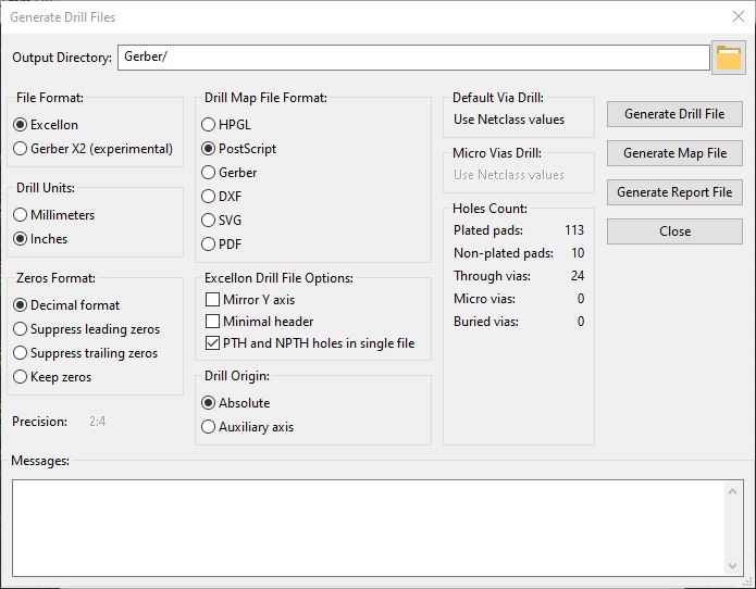
The Information about holes of the PCB is stored in a separate Drill File and to generate that I have used the above configuration for NextPCB. Other manufacturers may have different settings.
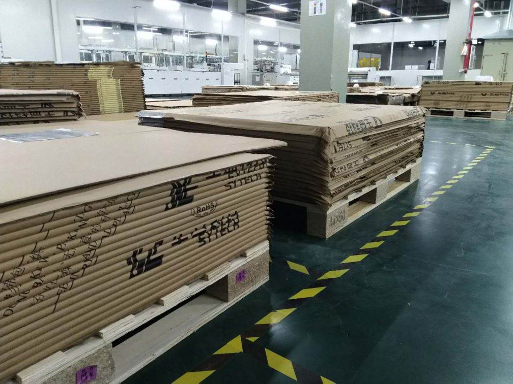
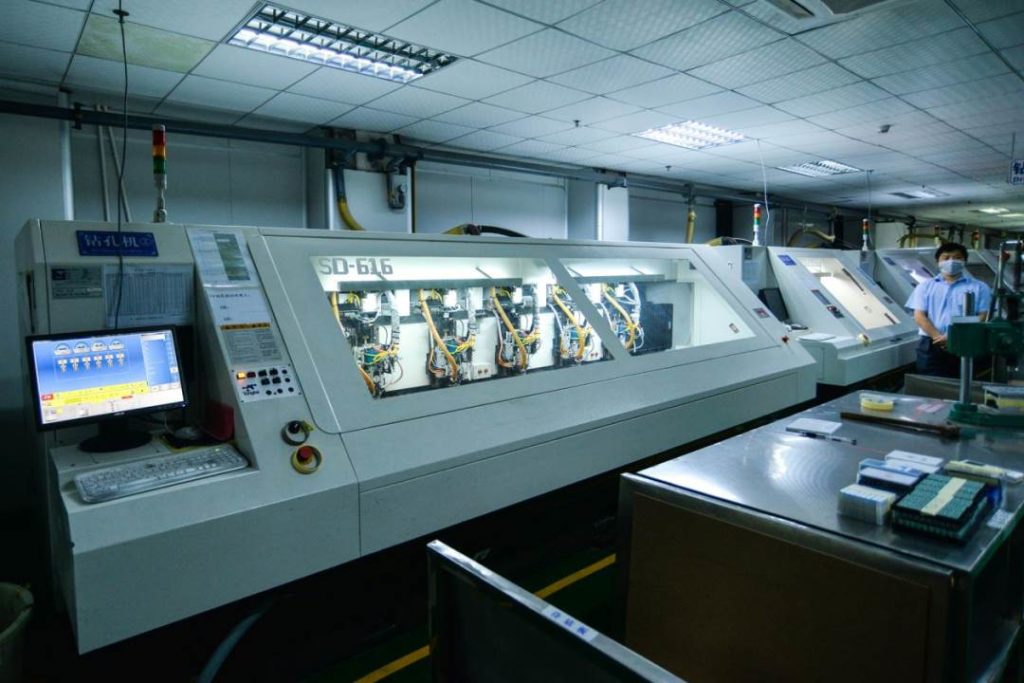
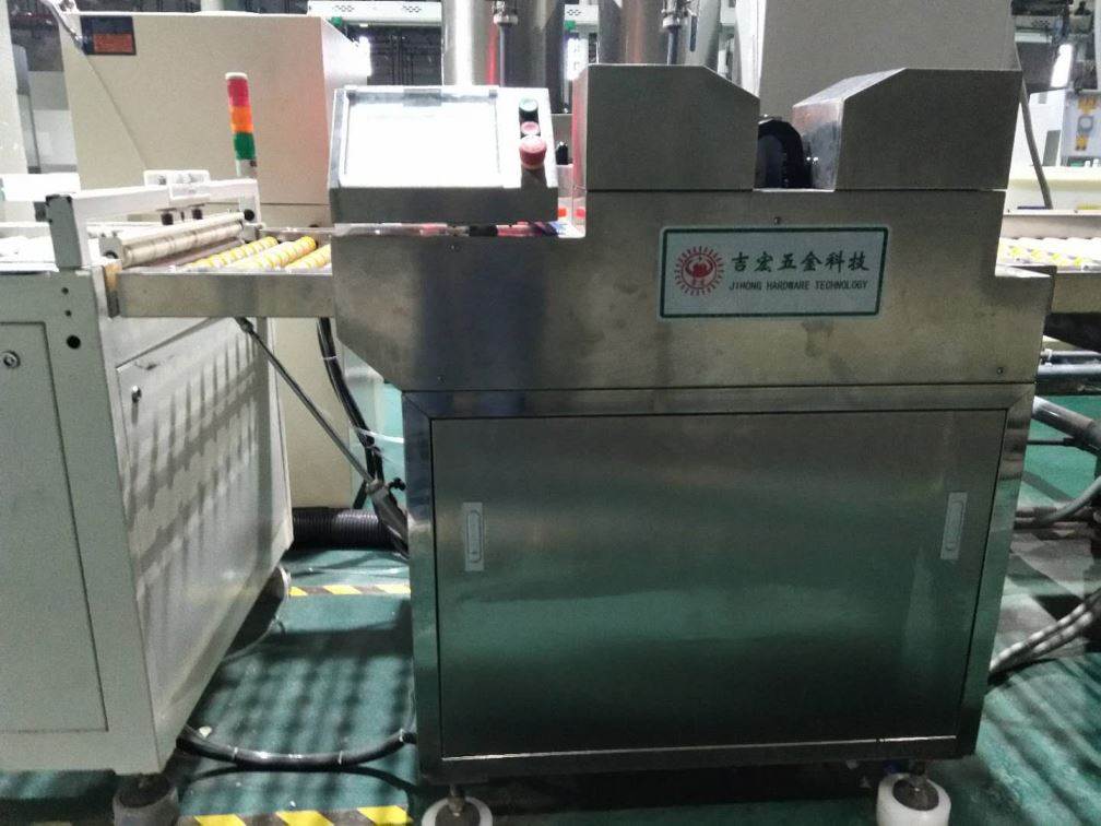
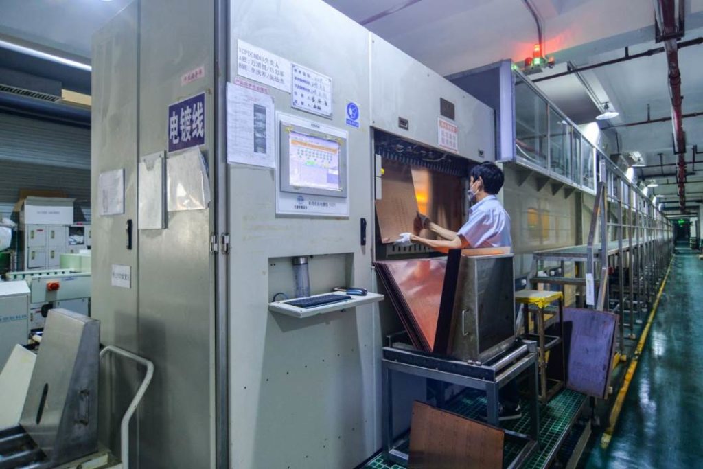
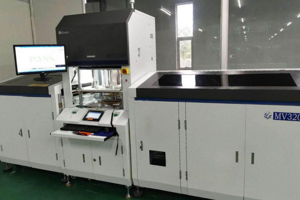
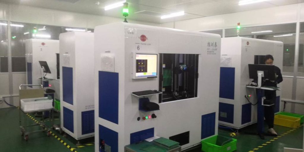
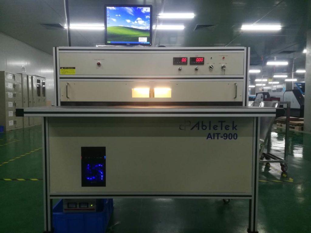
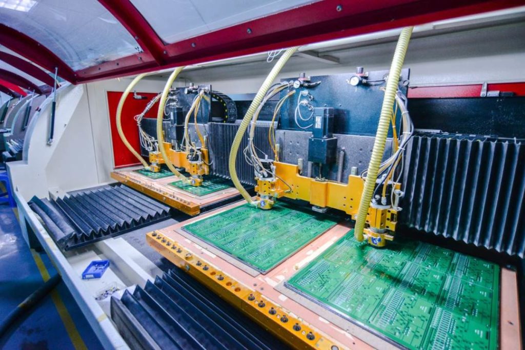
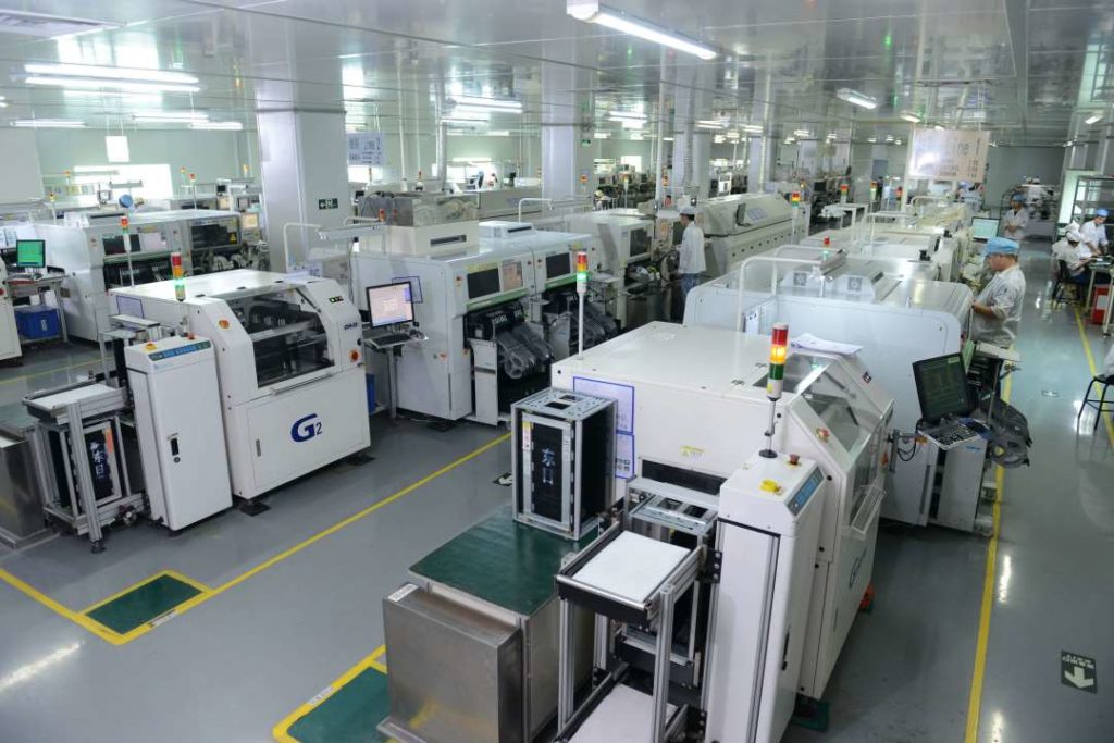
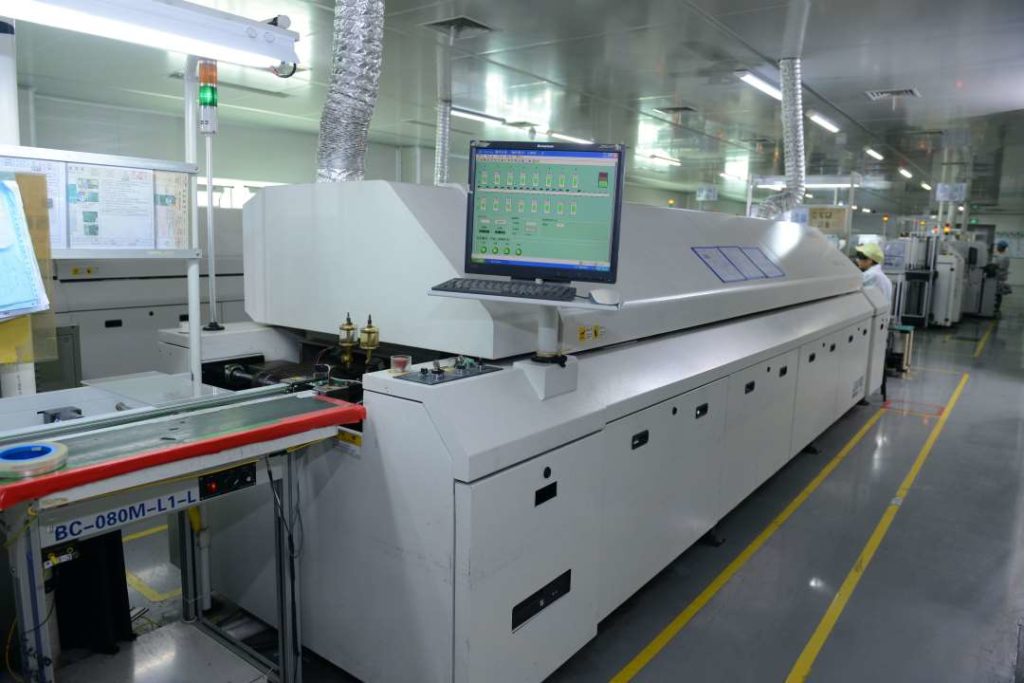
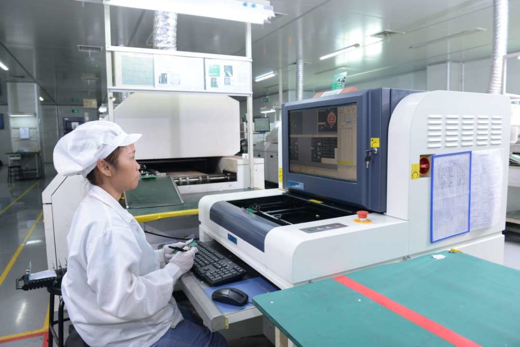
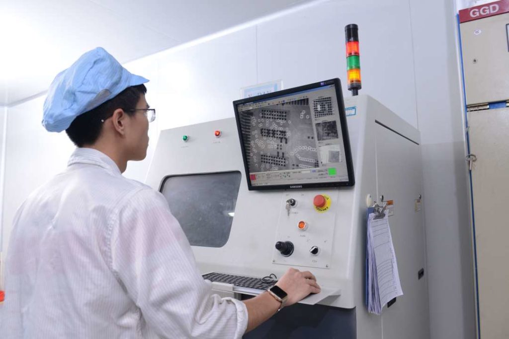
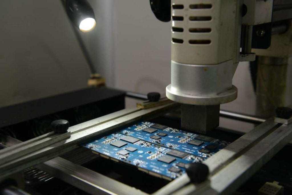
There are many reasons to select NextPCB one of the reason is their transparency about their manufacturing process. Below are some photos from their factory.
They also accept a variety of payment options : PayPal, Bank Transfer, Western Union, Cash Payment at HQ.
For the Shipping Methods, they have DHL, FedEx, Hongkong Post which is convenient with different prices and benefits.
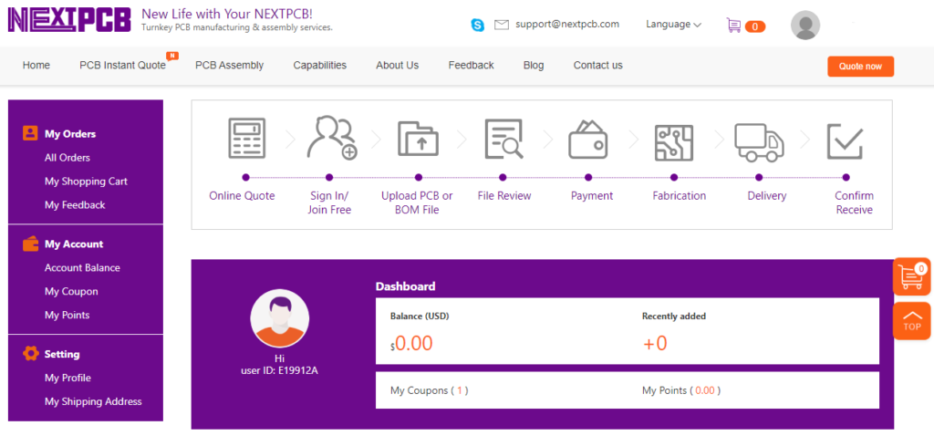
For the process of ordering, we need to create an account on the website. You can use the signup link and create a new account. after the account is created you will see something like below.
Next Step is to Upload your Gerber Files and place a successful order to begin the manufacturing. Once your Gerber is generated it is recommended to zip them together in a single file and upload them
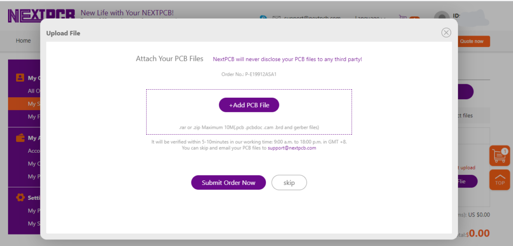
Once the Upload is finished you can see the order in your account page.
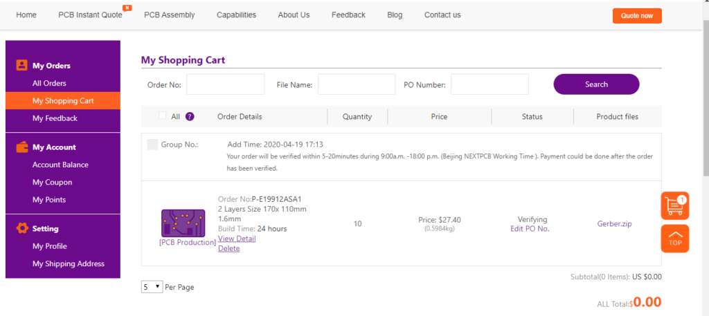
Your Order will be analysed properly and once it is ready for manufacturing they will ask for the payment and once the payment is cleared the manufacturing will be started.
They spend good effort in analyzing your Gerber Files as it may contain errors and may not manufacture well if the holes are too small or any other design errors in it.
If you are looking for a special discount you can use the Special Discount Offer button below. (Validation: Mar 26, 2020 – April 30, 2020)
Once the PCB is Verified and Manufactured you will receive the PCB in a few days and ready to be worked upon it.
Thank You for reading this article hope it helps you. Don’t forget to check other articles in this series.




0 Comments