Note
This article is a part of Arduino / ATmega328p Embedded C Firmware Programming Tutorial. Consider exploring the course home page for articles on similar topics.

Arduino Tutorial Embedded C Register Level Arduino Master Class
Also visit the Release Page for Register Level Embedded C Hardware Abstraction Library and Code for AVR.
Introduction
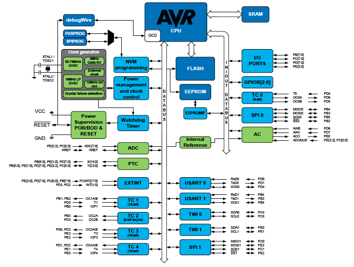
This article describes the different memories in the ATmega328P. The AVR memory architecture has two main memory spaces, the Data Memory and the Program Memory space. In addition, the ATmega328P features an EEPROM Memory for data storage. All three memory spaces are linear and regular.
AVR microcontrollers are built using a modified Harvard Architecture. This means the Flash Program Memory space is on a separate address bus than the Static Random Access Memory (SRAM). There are two data bus, one that can access all data and the In/Out data bus with limited access to a small section of memory.
What You Will Learn
- What is the internal Memory architecture of Arduino?
- What is the Memory map of AVR ATmega328p chip?
- How Flash, RAM and EEPROM is connected in ATmega328p?
- How is the IO Memory mapped in ATmega328p?
ATmega328P Flash Program Memory
The ATmega328P contains 32Kbytes On-chip In-System Reprogrammable Flash memory for program storage. Since all AVR instructions are 16 or 32 bits wide, the Flash is organized as 16K x 16. For software security, the Flash Program memory space is divided into two sections, Boot Loader Section and Application Program section.
The Flash memory has an endurance of at least 10,000 writes/erase cycles. The ATmega328P Program Counter (PC) is 14 bits wide and addresses the 16K program memory locations.
The Range of memory address for ATmega328P Flash Memory is 0x0000 – 0x3FFF.

ATmega328P SRAM Data Memory
Data can be accessed through the standard data bus (Load/Store Instructions). There is a secondary In/Out Bus for rapid direct access to select locations.
The ATmega328P is a complex microcontroller with more peripheral units than can be supported within the 64 locations reserved in the Opcode for the IN and OUT instructions. For the Extended I/O space from 0x60 – 0xFF in SRAM, only the ST/STS/STD (Store) and LD/LDS/LDD (Load) instructions can be used. The IN/OUT data bus has direct access to the 64-byte I/O Memory section (not Extended) using a 0x00 to 0x1F address. This memory can also be accessed by the standard data bus using a 0x20 address offset in the access command.
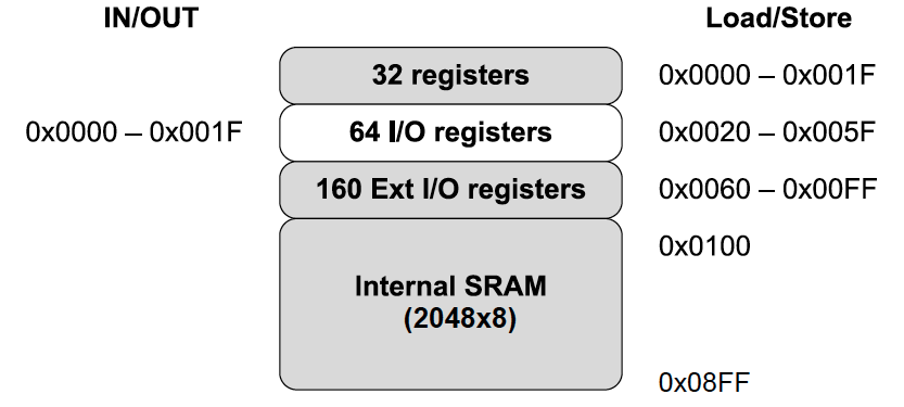
The ATmega328P Data Memory Address Space consists of The lower 2303 data memory locations address consists of the first 32 locations address the Register File, the next 64 location the standard I/O memory, then 160 locations of Extended I/O memory, and the next 2048 locations address the internal data SRAM.
- Registers (32 x 8-bit) (000016–001F16)
Consists of 32 8-bit general purpose working registers (R0-R31) - I/O Memory (64 x 8-bit) (002016–005F16)
Contains addressable space for peripheral control registers and other I/O registers - Extended I/O Memory (device dependent) (160 x 8-bit) (006016–00FF16)
Some AVR microcontrollers with more peripherals need more space than the I/O memory can address so some of the SRAM is used as Extended I/O memory to handle the extra peripherals control registers and other I/O functions - Internal SRAM (2048 x 8-bit) (010016–08FF16)
SRAM is used for temporarily storing intermediate results and variables, stack within a software application.
There are five different data bus addressing modes for the data memory:
- Direct – The direct addressing reaches the entire data space.
- Indirect – In the Register File, registers R26 to R31 feature the indirect addressing pointer registers.
- Indirect with Displacement – The Indirect with Displacement mode reaches 63 address locations from the base address given by the Y or Z register.
- Indirect with Pre-decrement – The address registers X, Y, and Z are decremented.
- Indirect with Post-increment – The address registers X, Y, and Z are incremented.
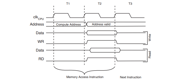
The internal data SRAM access takes two clkCPU cycles.
ATmega328P EEPROM Data Memory
The ATmega328P contains 1Kbytes of data EEPROM memory. It is organized as a separate data space, in which single bytes can be read and written. The EEPROM has an endurance of at least 100,000 writes/erase cycles. The access between the EEPROM and the CPU is performed using the EEPROM Address Registers, the EEPROM Data Register, and the EEPROM Control Register. The EEPROM Access Registers are accessible in the I/O space.
In order to prevent unintentional EEPROM writes, a specific write procedure must be followed to reduce wear. An EEPROM write takes 3.4ms to Erase and Write in one operation (Atomic Operation). 1.8ms to Erase Only and 1.8ms to Write Only. When the EEPROM is read, the CPU is halted for four clock cycles before the next instruction is executed. The EEPROM read access takes one instruction, and the requested data is available immediately. When the EEPROM is written, the CPU is halted for two clock cycles before the next instruction is executed.
During periods of low VCC, the EEPROM data can be corrupted because the supply voltage is too low for the CPU and the EEPROM to operate properly. These issues are the same as for board level systems using EEPROM, and the same design solutions should be applied.
ATmega328P Input/Output (I/O) Memory
ATmega328P I/Os and peripherals are placed in the I/O space. All I/O locations may be accessed by the LD/LDS/LDD and ST/STS/STD instructions, transferring data between the 32 general purpose working registers and the I/O space. I/O Registers within the address range 0x00 – 0x1F are directly bit-accessible using the SBI and CBI instructions. In these registers, the value of single bits can be checked by using the SBIS and SBIC instructions. When using the I/O specific commands IN and OUT, the I/O addresses 0x00 – 0x3F must be used. When addressing I/O Registers as data space using LD and ST instructions, 0x20 must be added to these addresses. The ATmega328/P is a complex microcontroller with more peripheral units than can be supported within the 64 locations reserved in Opcode for the IN and OUT instructions. For the Extended I/O space from 0x60 – 0xFF in SRAM, only the ST/STS/STD, and LD/LDS/LDD instructions can be used.
| Address I/O (L/S) | Name | Bit 7 | Bit 6 | Bit 5 | Bit 4 | Bit 3 | Bit 2 | Bit 1 | Bit 0 | Page |
|---|---|---|---|---|---|---|---|---|---|---|
| 0x1F (0x3F) | EECR | – | – | EEPM1 | EEPM0 | EERIE | EEMPE | EEPE | EERE | 21 |
| 0x1E (0x3E) | GPIOR0 | 15 | ||||||||
| 0x1D (0x3D) | EIMSK | – | – | – | – | – | – | INT1 | INT0 | 73 |
| 0x1C (0x3C) | EIFR | – | – | – | – | – | – | INTF1 | INTF0 | 73 |
| 0x1B (0x3B) | PCIFR | – | – | – | – | – | PCIF2 | PCIF1 | PCIF0 | |
| 0x17 (0x37) | TIFR2 | – | – | – | – | – | OCF2B | OCF2A | TOV2 | 160 |
| 0x16 (0x36) | TIFR1 | – | – | ICF1 | – | – | OCF1B | OCF1A | TOV1 | 137 |
| 0x15 (0x35) | TIFR0 | – | – | – | – | – | OCF0B | OCF0A | TOV0 | |
| 0x0B (0x2B) | PORTD | PORTD7 | PORTD6 | PORTD5 | PORTD4 | PORTD3 | PORTD2 | PORTD1 | PORTD0 | 93 |
| 0x0A (0x2A) | DDRD | DDD7 | DDD6 | DDD5 | DDD4 | DDD3 | DDD2 | DDD1 | DDD0 | 93 |
| 0x09 (0x29) | PIND | PIND7 | PIND6 | PIND5 | PIND4 | PIND3 | PIND2 | PIND1 | PIND0 | 93 |
| 0x08 (0x28) | PORTC | – | PORTC6 | PORTC5 | PORTC4 | PORTC3 | PORTC2 | PORTC1 | PORTC0 | 92 |
| 0x07 (0x27) | DDRC | – | DDC6 | DDC5 | DDC4 | DDC3 | DDC2 | DDC1 | DDC0 | 92 |
| 0x06 (0x26) | PINC | – | PINC6 | PINC5 | PINC4 | PINC3 | PINC2 | PINC1 | PINC0 | 92 |
| 0x05 (0x25) | PORTB | PORTB7 | PORTB6 | PORTB5 | PORTB4 | PORTB3 | PORTB2 | PORTB1 | PORTB0 | 92 |
| 0x04 (0x24) | DDRB | DDB7 | DDB6 | DDB5 | DDB4 | DDB3 | DDB2 | DDB1 | DDB0 | 92 |
| 0x03 (0x23) | PINB | PINB7 | PINB6 | PINB5 | PINB4 | PINB3 | PINB2 | PINB1 | PINB0 | 92 |
| Address | Name | Bit 7 | Bit 6 | Bit 5 | Bit 4 | Bit 3 | Bit 2 | Bit 1 | Bit 0 | Page |
ATmega328P General Purpose I/O Registers
The ATmega328P contains three General Purpose I/O Registers. These registers can be used for storing any information, and they are particularly useful for storing global variables and Status Flags. General Purpose I/O Registers within the address range 0x00 – 0x1F are directly bit-accessible using the SBI, CBI, SBIS, and SBIC instructions.
GPIOR2 – General Purpose I/O Register 2
| Bit | 7 | 6 | 5 | 4 | 3 | 2 | 1 | 0 |
| 0x2B (0x4B) | MSB | LSB | ||||||
| Read/Write | R/W | R/W | R/W | R/W | R/W | R/W | R/W | R/W |
| Initial Value | 0 | 0 | 0 | 0 | 0 | 0 | 0 | 0 |
GPIOR1 – General Purpose I/O Register 1
| Bit | 7 | 6 | 5 | 4 | 3 | 2 | 1 | 0 |
| 0x2A (0x4A) | MSB | LSB | ||||||
| Read/Write | R/W | R/W | R/W | R/W | R/W | R/W | R/W | R/W |
| Initial Value | 0 | 0 | 0 | 0 | 0 | 0 | 0 | 0 |
GPIOR0 – General Purpose I/O Register 0
| Bit | 7 | 6 | 5 | 4 | 3 | 2 | 1 | 0 |
| 0x1E (0x3E) | MSB | LSB | ||||||
| Read/Write | R/W | R/W | R/W | R/W | R/W | R/W | R/W | R/W |
| Initial Value | 0 | 0 | 0 | 0 | 0 | 0 | 0 | 0 |


0 Comments