Note
This article is a part of Arduino / ATmega328p Embedded C Firmware Programming Tutorial. Consider exploring the course home page for articles on similar topics.

Arduino Tutorial Embedded C Register Level Arduino Master Class
Also visit the Release Page for Register Level Embedded C Hardware Abstraction Library and Code for AVR.
Introduction
GPIO (General Purpose Input/Output) is a software controlled interface that is usually found on Microcontrollers and some Microprocessor ICs or interface chipsets. Typically, the GPIO is one or more pins on the IC which have no special purpose in themselves, but which facilitate an optional ability for device designers to create an interface/connection between the IC and a peripheral component by programming some hardware registers. Thereby, within limitations, GPIO pins can be tailored for use to provide some specific function or purpose within a hardware device design.
System-on-Chip (SOC) processors, Microcontrollers, DSP, etc heavily rely on GPIOs. In some cases, every non-dedicated pin can be configured as a GPIO; and most chips have at least several dozens of them. Programmable logic devices (like FPGAs) can easily provide GPIOs; multifunction chips like power managers and audio codecs often have a few such pins to help with pin scarcity on SOCs, and there are also “GPIO Expander” chips that connect using the I2C or SPI serial buses. GPIO Pins are also seen in ICs like PMICs, LED Controllers, etc.
Some basic GPIO capabilities are :
- GPIO Pins can be enabled or disabled as needed
- Output values are writable (high=1, low=0)
- Input values are readable (high=1, low=0)
- Inputs can often be used as IRQ (Interrupt Request) signals, Edge triggered or Level triggered. Such IRQs may be configurable to wake the system from a low power state
What You Will Learn
- How the GIPO work in Arduino?
- How the IO Ports work in AVR ATmega328p?
- What are the modes of IO Port in Arduino/ATmega328p?
GPIO Input Output Modes
- High Impedance / Floating / Hi-Z / Tri-Stated
- Input Mode with Pull-Up or Pull-Down
- Output Mode with Open Drain
- Output Mode with Push Pull
High Impedance / Floating / Hi-Z / Tri-Stated
When a GPIO pin is put into a High Impedance state it effectively gets disconnected from the external interface. The basic concept of the third state, high impedance (Hi-Z), is to effectively remove the device’s influence from the rest of the circuit. If more than one device is electrically connected to another device, putting a pin into the Hi-Z state is often used to prevent short circuits, or one device driving high (logical 1) against another device driving low (logical 0).

A tri-state buffer can be thought of as a switch. If B is on, the switch is closed. If B is off, the switch is open. Credit
It is unsafe to keep pins floating as it will lead to leakage current and in turn cause high power consumption and electrical noise problem.
Input Mode with Pull-Up or Pull-Down
When a GPIO pin is used with an Internal or External Pull -Up or Pull-Down Resistor to ensure a known state of logic. It is used typically with a switch or input device such that whenever the switch is pressed or input comes it toggles the logic level.
Pull-Up ensures a well-defined Logic Level of High = 1. A Pull-Up resistor usually connects the pin to Vcc. It holds the logic too High when no other active input comes.
Pull-Down ensures a well-defined Logic Level of Low = 1. A Pull-Down resistor usually connects the pin to GND. It holds the logic to Low when no other active input comes.

When the switch is open the voltage of the gate input is pulled up to the level of Vin. When the switch is closed, the input voltage at the gate goes to the ground.
When the switch is open, the voltage across a pull-up resistor with sufficiently low impedance vanishes to the effect that it looks like a wire to VCC. On the other hand, when the switch is closed, the pull-up resistor must have a sufficiently high impedance in comparison to the closed switch to not affect the connection to the ground. Together, these two conditions can be used to derive an appropriate value for the impedance of the pull-up resistor but usually, only a lower bound is derived assuming that the critical components do indeed have infinite impedance.
Many microcontrollers have internal programmable Pull-Up or Down resistors that can be enabled or disabled based on the need or application. This works as an advantage as it removes the cost of external resistors and complexity.
Unused pins are recommended to be kept in either Pull-Up or Pull-Down state as this will hold the Logic Level of the pin and stop any leakage current and voltage fluctuations.
Output Mode with Open Drain
An Open Drain output can take two states Low Impedance and High Impedance. In a Low Impedance state, it can sink current. It is like a switch that is either connected to the ground or open.
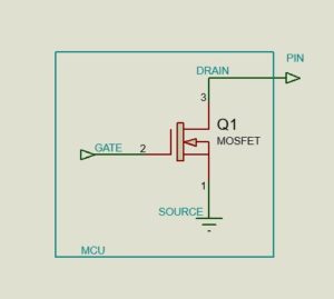
The MOSFET has three terminals called: gate, source, and drain. In an open-drain configuration, the source is grounded, the gate is driven internally, and the drain is the pin (i.e. not connected to external hardware). When the Gate is driven, Drain gets connected with the Source and the PIN gets a Logic Low = 0. Otherwise, the PIN remains at High-Z state which is useless until a Pull-Up is used.
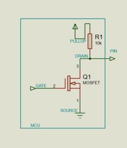
In order to achieve a logically high output on the line, a pull-up resistor is used to connect the open-drain output to the desired output voltage level.
I2C Bus uses SDA and SCL Pins in Open Drain Configuration thus it need Pull Up resistors to achieve a logic High. The value of resistance depends on Bus Length, Capacitance, Clock Frequency, etc. Usually it is between 4.7K Ohm to 10K Ohm.
Output Mode with Push Pull
A Push-Pull output is capable of both sourcing and sinking current.
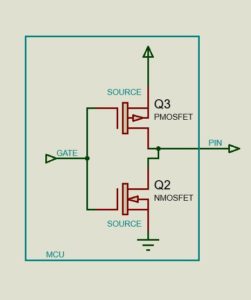
When the top transistor [PMOS] will be activated, the output PIN will be HIGH and act as a Source. When the NMOS below will be on, the output PIN is driven LOW and act as a Sink. It is a complementary logic and only once MOS will be activated at a time.
0 Comments