Note
This article is a part of Arduino / ATmega328p Embedded C Firmware Programming Tutorial. Consider exploring the course home page for articles on similar topics.

Arduino Tutorial Embedded C Register Level Arduino Master Class
Also visit the Release Page for Register Level Embedded C Hardware Abstraction Library and Code for AVR.
Introduction
Atmega328p is used as an example to explain the concepts but they are applicable to all the AVR 8-bit Microcontrollers.
All AVR ports have true Read-Modify-Write functionality when used as general digital I/O ports. This means that the direction of one port pin can be changed without unintentionally changing the direction of any other pin with the SBI and CBI instructions. The same applies when changing drive value (if configured as an output) or enabling/disabling pull-up resistors (if configured as input). Each output buffer has symmetrical drive characteristics with both high sink and source capability. The pin driver is strong enough to drive LED displays directly. All port pins have individually selectable pull-up resistors with a supply-voltage invariant resistance. All I/O pins have protection diodes to both VCC and Ground.
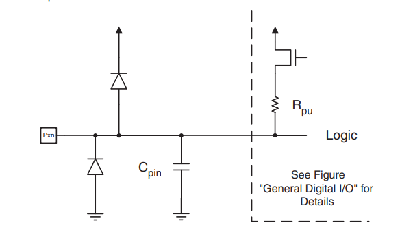
All registers and bit references in this section are written in a general form. A lower case “x” represents the numbering letter for the port, and a lower case “n” represents the bit number. However, when using the register or bit defines in a program, the precise form must be used. For example, PORTB3 for a bit no. 3 in Port B, here documented generally as PORTxn.
Three I/O memory address locations are allocated for each port, one each for
- Data Register – PORTx – Read Write
- Data Direction Register – DDRx – Read Write
- Port Input Pins – PINx – Read Only
What You Will Learn
- What are the IO Port Registers in Arduino?
- What are the GPIO Registers in AVR ATmega328p?
- Which AVR Registers control and configures Digital Input Output?
- What is the function of the PORT, DDR and PIN Registers?
Ports as General Digital I/O
The ports are bi-directional I/O ports with optional internal pull-ups.
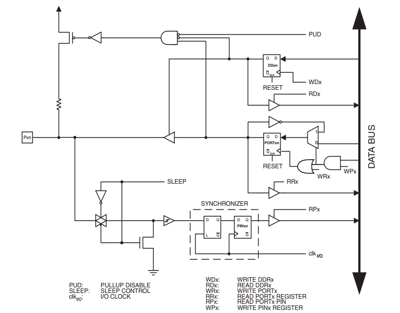
WRx, WPx, WDx, RRx, RPx, and RDx are common to all pins within the same port. clkI/O, SLEEP, and PUD are common to all ports
The DDxn bit in the DDRx Register selects the direction of this pin. If DDxn is written logic one, Pxn is configured as an output pin. If DDxn is written logic zero, Pxn is configured as an input pin.
| DDRB | 7 | 6 | 5 | 4 | 3 | 2 | 1 | 0 |
| 0x04 (0x24) | DDRB7 | DDRB6 | DDRB5 | DDRB4 | DDRB3 | DDRB2 | DDRB1 | DDRB0 |
| Read/Write | R/W | R/W | R/W | R/W | R/W | R/W | R/W | R/W |
| Initial Value | 0 | 0 | 0 | 0 | 0 | 0 | 0 | 0 |
| DDRC | 7 | 6 | 5 | 4 | 3 | 2 | 1 | 0 |
| 0x07 (0x27) | DDRC7 | DDRC6 | DDRC5 | DDRC4 | DDRC3 | DDRC2 | DDRC1 | DDRC0 |
| Read/Write | R/W | R/W | R/W | R/W | R/W | R/W | R/W | R/W |
| Initial Value | 0 | 0 | 0 | 0 | 0 | 0 | 0 | 0 |
| DDRD | 7 | 6 | 5 | 4 | 3 | 2 | 1 | 0 |
| 0x0A (0x2A) | DDRD7 | DDRD6 | DDRD5 | DDRD4 | DDRD3 | DDRD2 | DDRD1 | DDRD0 |
| Read/Write | R/W | R/W | R/W | R/W | R/W | R/W | R/W | R/W |
| Initial Value | 0 | 0 | 0 | 0 | 0 | 0 | 0 | 0 |
If PORTxn is written logic one when the pin is configured as an input pin, the pull-up resistor is activated. To switch the pull-up resistor off, PORTxn has to be written logic zero, or the pin has to be configured as an output pin. The port pins are tri-stated when the reset condition becomes active, even if no clocks are running.
If PORTxn is written logic one when the pin is configured as an output pin, the port pin is driven high (one). If PORTxn is written logic zero when the pin is configured as an output pin, the port pin is driven low (zero).
| PORTB | 7 | 6 | 5 | 4 | 3 | 2 | 1 | 0 |
| 0x05 (0x25) | PORTB7 | PORTB6 | PORTB5 | PORTB4 | PORTB3 | PORTB2 | PORTB1 | PORTB0 |
| Read/Write | R/W | R/W | R/W | R/W | R/W | R/W | R/W | R/W |
| Initial Value | 0 | 0 | 0 | 0 | 0 | 0 | 0 | 0 |
| PORTC | 7 | 6 | 5 | 4 | 3 | 2 | 1 | 0 |
| 0x08 (0x28) | PORTC7 | PORTC6 | PORTC5 | PORTC4 | PORTC3 | PORTC2 | PORTC1 | PORTC0 |
| Read/Write | R/W | R/W | R/W | R/W | R/W | R/W | R/W | R/W |
| Initial Value | 0 | 0 | 0 | 0 | 0 | 0 | 0 | 0 |
| PORTD | 7 | 6 | 5 | 4 | 3 | 2 | 1 | 0 |
| 0x0B (0x2B) | PORTD7 | PORTD6 | PORTD5 | PORTD4 | PORTD3 | PORTD2 | PORTD1 | PORTD0 |
| Read/Write | R/W | R/W | R/W | R/W | R/W | R/W | R/W | R/W |
| Initial Value | 0 | 0 | 0 | 0 | 0 | 0 | 0 | 0 |
Writing a logic one to PINxn toggles the value of PORTxn, independent of the value of DDRxn. Note that the SBI instruction can be used to toggle one single bit in a port.
Independent of the setting of Data Direction bit DDxn, the port pin can be read through the PINxn Register bit.
| PINB | 7 | 6 | 5 | 4 | 3 | 2 | 1 | 0 |
| 0x03 (0x23) | PINB7 | PINB6 | PINB5 | PINB4 | PINB3 | PINB2 | PINB1 | PINB0 |
| Read/Write | R/W | R/W | R/W | R/W | R/W | R/W | R/W | R/W |
| Initial Value | N/A | N/A | N/A | N/A | N/A | N/A | N/A | N/A |
| PINC | 7 | 6 | 5 | 4 | 3 | 2 | 1 | 0 |
| 0x06 (0x26) | PINC7 | PINC6 | PINC5 | PINC4 | PINC3 | PINC2 | PINC1 | PINC0 |
| Read/Write | R/W | R/W | R/W | R/W | R/W | R/W | R/W | R/W |
| Initial Value | N/A | N/A | N/A | N/A | N/A | N/A | N/A | N/A |
| PIND | 7 | 6 | 5 | 4 | 3 | 2 | 1 | 0 |
| 0x09 (0x29) | PIND7 | PIND6 | PIND5 | PIND4 | PIND3 | PIND2 | PIND1 | PIND0 |
| Read/Write | R/W | R/W | R/W | R/W | R/W | R/W | R/W | R/W |
| Initial Value | N/A | N/A | N/A | N/A | N/A | N/A | N/A | N/A |
//Refer the table above
unsigned char i;
...
/* Define pull-ups and set outputs high */
/* Define directions for port pins */
PORTB = (1<<PB7)|(1<<PB6)|(1<<PB1)|(1<<PB0);
DDRB = (1<<DDB3)|(1<<DDB2)|(1<<DDB1)|(1<<DDB0);
/* Insert nop for synchronization*/
__no_operation();
/* Read port pins */
i = PINB;
...
If some pins are unused, it is recommended to ensure that these pins have a defined level. Even though most of the digital inputs are disabled in the deep sleep modes as described above, floating inputs should be avoided to reduce current consumption in all other modes where the digital inputs are enabled (Reset, Active mode, and Idle mode).
The simplest method to ensure a defined level of an unused pin is to enable the internal pull-up. In this case, the pull-up will be disabled during the reset. If low power consumption during reset is important, it is recommended to use an external pull-up or pull-down. Connecting unused pins directly to VCC or GND is not recommended, since this may cause excessive currents if the pin is accidentally configured as an output.
| DDxn | PORTxn |
PUD (in MCUCR) | I/O | Pull-up | Comment |
| 0 | 0 | X | Input | No | Tri-state (Hi-Z) |
| 0 | 1 | 0 | Input | Yes | Pxn will source current if ext. pulled low |
| 0 | 1 | 1 | Input | No | Tri-state (Hi-Z) |
| 1 | 0 | X | Output | No | Output Low (Sink) |
| 1 | 1 | X | Output | No | Output High (Source) |
MCUCR – MCU Control Register
| MCUCR | 7 | 6 | 5 | 4 | 3 | 2 | 1 | 0 |
| 0x35 (0x24) | – | BODS | BODSE | PUD | – | – | IVSEL | IVCE |
| Read/Write | R | R/W | R/W | R/W | R | R | R/W | R/W |
| Initial Value | 0 | 0 | 0 | 0 | 0 | 0 | 0 | 0 |
• Bit 4 – PUD: Pull-up Disable
When this bit is written to one, the pull-ups in the I/O ports are disabled even if the DDxn and PORTxn Registers are configured to enable the pull-ups ({DDxn, PORTxn} = 0b01).


0 Comments