Note
This article is a part of Arduino / ATmega328p Embedded C Firmware Programming Tutorial. Consider exploring the course home page for articles on similar topics.

Arduino Tutorial Embedded C Register Level Arduino Master Class
Also visit the Release Page for Register Level Embedded C Hardware Abstraction Library and Code for AVR.
Introduction
This section discusses the Atmega328p and Arduino Pinout and Mapping. The Arduino style pinout is mapped with the chip style pinout and the alternate functions are described.
Most port pins have alternate functions in addition to being general digital I/Os. The below article shows and discusses the peripheral available in each port pin and their alternate functions.
What You Will Learn
- What are the different pins in Arduino UNO?
- What are the pin configuration of AVR ATmega328p chip?
- How many ports are there in ATmega328p?
- What are the alternate function of each Arduino pin?
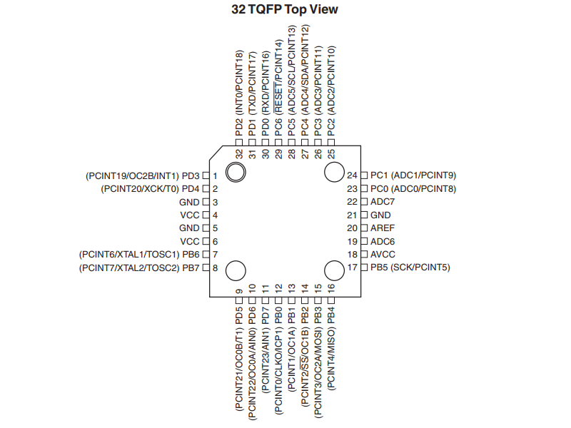
ATmega328P Pin Configuration / PinOut
Below are the two most popular packages of ATmega328P that are sold and used in Arduino Board. Arduino UNO uses the PDIP package of ATmega328P and Arduino NANO uses the TQFP Package of ATmega328P.
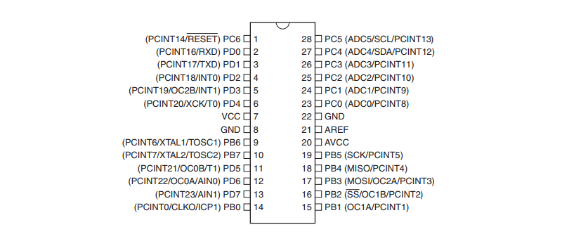
Pin Description ATmega328P
VCC
Digital Supply Voltage for the operation of the chip.
GND
Digital Supply Ground for the operation of the chip.
AVCC
AVCC is the supply voltage pin for the A/D Converter, PC3:0, and ADC7:6. It should be externally connected to VCC, even if the ADC is not used. If the ADC is used, it should be connected to VCC through a low-pass filter. Note that PC6…4 use digital supply voltage, VCC.
AREF
AREF is the analog reference pin for the A/D Converter.
ADC7:6 (TQFP and QFN/MLF Package Only) (D21:D20 Arduino NANO)
In the TQFP and QFN/MLF package, ADC7:6 serves as analog inputs to the A/D converter. These pins are powered from the analog supply and serve as 10-bit ADC channels.
Port B (PB7:0)
Port B is an 8-bit bi-directional I/O port with internal pull-up resistors (selected for each bit). The Port B output buffers have symmetrical drive characteristics with both high sink and source capability. As inputs, Port B pins that are externally pulled low will source current if the pull-up resistors are activated. The Port B pins are tri-stated when a reset condition becomes active, even if the clock is not running.
Depending on the clock selection fuse settings, PB6 can be used as input to the inverting Oscillator amplifier and input to the internal clock operating circuit.
Depending on the clock selection fuse settings, PB7 can be used as output from the inverting Oscillator amplifier.
If the Internal Calibrated RC Oscillator is used as the chip clock source, PB7…6 is used as TOSC2…1 input for the Asynchronous Timer/Counter2 if the AS2 bit in ASSR is set.
| Port Pin | Arduino Pin | Alternate Functions |
|---|---|---|
| PB7 | XTAL2 (Chip Clock Oscillator pin 2) Used as clock pin for Crystal Oscillator or Low-frequency Crystal Oscillator. When used as a clock pin, the pin can not be used as an I/O pin. TOSC2 (Timer Oscillator pin 2) In this mode, a crystal Oscillator is connected to this pin and used for asynchronous clocking of Timer/Counter2 and the pin cannot be used as an I/O pin. PCINT7 (Pin Change Interrupt 7) The PB7 pin can serve as an external interrupt source. | |
| PB6 | XTAL1 (Chip Clock Oscillator pin 1 or External clock input) Used for all chip clock sources except internal calibrated RC Oscillator. When used as a clock pin, the pin can not be used as an I/O pin. TOSC1 (Timer Oscillator pin 1) In this mode, a crystal Oscillator is connected to this pin and used for asynchronous clocking of Timer/Counter1 and the pin cannot be used as an I/O pin. PCINT6 (Pin Change Interrupt 6) The PB6 pin can serve as an external interrupt source. | |
| PB5 | D13 | SCK (SPI Bus Master clock Input) When the SPI is enabled as a Slave, this pin is configured as an input regardless of the setting of DDB5. When the SPI is enabled as a Master, the data direction of this pin is controlled by DDB5. PCINT5 (Pin Change Interrupt 5) The PB5 pin can serve as an external interrupt source. |
| PB4 | D12 | MISO (SPI Bus Master Input/Slave Output) When the SPI is enabled as a Master, this pin is configured as an input regardless of the setting of DDB4. When the SPI is enabled as a Slave, the data direction of this pin is controlled by DDB4. PCINT4 (Pin Change Interrupt 4) The PB4 pin can serve as an external interrupt source. |
| PB3 | D11 | MOSI (SPI Bus Master Output/Slave Input) When the SPI is enabled as a Slave, this pin is configured as an input regardless of the setting of DDB3. When the SPI is enabled as a Master, the data direction of this pin is controlled by DDB3. OC2A (Timer/Counter2 Output Compare Match A Output) This pin can serve as an external output for the Timer/Counter2 in Compare Match mode or PWM mode. PCINT3 (Pin Change Interrupt 3) The PB3 pin can serve as an external interrupt source. |
| PB2 | D10 | SS (SPI Bus Master Slave select) When the SPI is enabled as a Slave, this pin is configured as an input regardless of the setting of DDB2. When the SPI is enabled as a Master, the data direction of this pin is controlled by DDB2. OC1B (Timer/Counter1 Output Compare Match B Output) This pin can serve as an external output for the Timer/Counter1 in Compare Match mode or PWM mode. PCINT2 (Pin Change Interrupt 2) The PB2 pin can serve as an external interrupt source. |
| PB1 | D9 | OC1A (Timer/Counter1 Output Compare Match A Output) This pin can serve as an external output for the Timer/Counter1 in Compare Match mode or PWM mode. PCINT1 (Pin Change Interrupt 1) The PB1 pin can serve as an external interrupt source. |
| PB0 | D8 | ICP1 (Timer/Counter1 Input Capture Input) The PB0 pin can act as an Input Capture Pin for Timer/Counter1. CLKO (Divided System Clock Output) The divided system clock can be output on the PB0 pin. It will also be output during reset. PCINT0 (Pin Change Interrupt 0) The PB0 pin can serve as an external interrupt source. |
| Port Pin | Arduino Pin | Alternate Function |
Port C (PC5:0)
Port C is a 7-bit bi-directional I/O port with internal pull-up resistors (selected for each bit). The PC5…0 output buffers have symmetrical drive characteristics with both high sink and source capability. As inputs, Port C pins that are externally pulled low will source current if the pull-up resistors are activated. The Port C pins are tri-stated when a reset condition becomes active, even if the clock is not running.
| Port Pin | Arduino Pin | Alternate Function |
|---|---|---|
| PC6 | RESET | RESET (Reset pin) When the RSTDISBL Fuse is programmed, this pin functions as a normal I/O pin, and ATmega328P will have to rely on Power-on Reset and Brown-out Reset as its reset sources. When the RSTDISBL Fuse is unprogrammed, the reset circuitry is connected to the pin, and the pin can not be used as an I/O pin. PCINT14 (Pin Change Interrupt 14) The PC6 pin can serve as an external interrupt source. |
| PC5 | A5 / D19 | ADC5 (ADC Input Channel 5) PC5 can also be used as ADC input Channel 5. Note that ADC input channel 5 uses digital power (VCC). SCL (2-wire Serial Bus Clock Line) When the 2-wire Serial Interface (I2C) is enabled the PC5 pin is disconnected from the port and becomes the Serial Clock I/O pin for the 2-wire Serial Interface. PCINT13 (Pin Change Interrupt 13) The PC5 pin can serve as an external interrupt source. |
| PC4 | A4 / D18 | ADC4 (ADC Input Channel 4) PC5 can also be used as ADC input Channel 4. Note that ADC input channel 5 uses digital power (VCC). SDA (2-wire Serial Bus Data Input/Output Line) When the 2-wire Serial Interface (I2C) is enabled the PC5 pin is disconnected from the port and becomes the Serial Data I/O pin for the 2-wire Serial Interface. PCINT12 (Pin Change Interrupt 12) The PC4 pin can serve as an external interrupt source. |
| PC3 | A3 / D17 | ADC3 (ADC Input Channel 3) PC3 can also be used as ADC input Channel 3. Note that ADC input channel 3 uses analog power (AVCC). PCINT11 (Pin Change Interrupt 11) The PC3 pin can serve as an external interrupt source. |
| PC2 | A2 / D16 | ADC2 (ADC Input Channel 2) PC2 can also be used as ADC input Channel 2. Note that ADC input channel 3 uses analog power (AVCC). PCINT10 (Pin Change Interrupt 10) The PC2 pin can serve as an external interrupt source. |
| PC1 | A1 / D15 | ADC1 (ADC Input Channel 1) PC1 can also be used as ADC input Channel 1. Note that ADC input channel 3 uses analog power (AVCC). PCINT9 (Pin Change Interrupt 9) The PC1 pin can serve as an external interrupt source. |
| PC0 | A0 / D14 | ADC0 (ADC Input Channel 0) PC0 can also be used as ADC input Channel 0. Note that ADC input channel 3 uses analog power (AVCC). PCINT8 (Pin Change Interrupt 8) The PC0 pin can serve as an external interrupt source. |
| Port Pin | Arduino Pin | Alternate Function |
PC6/ ~RESET
If the RSTDISBL Fuse is programmed, PC6 is used as an I/O pin. Note that the electrical characteristics of PC6 differ from those of the other pins of Port C.
If the RSTDISBL Fuse is unprogrammed, PC6 is used as a Reset input. A low level on this pin for longer than the minimum pulse length (2.5µs) will generate a Reset, even if the clock is not running.
Port D (PD7:0)
Port D is an 8-bit bi-directional I/O port with internal pull-up resistors (selected for each bit). The Port D output buffers have symmetrical drive characteristics with both high sink and source capability. As inputs, Port D pins that are externally pulled low will source current if the pull-up resistors are activated. The Port D pins are tri-stated when a reset condition becomes active, even if the clock is not running.
| Port Pin | Arduino Pin | Alternate Function |
|---|---|---|
| PD7 | D7 | AIN1 (Analog Comparator Negative Input) Analog Comparator Negative Input Pin. Configure internal pull-up switched off and port pin as an input. PCINT23 (Pin Change Interrupt 23) The PD7 pin can serve as an external interrupt source. |
| PD6 | D6 | AIN0 (Analog Comparator Positive Input) Analog Comparator Positive Input Pin. Configure internal pull-up switched off and port pin as an input. OC0A (Timer/Counter0 Output Compare Match A Output) This pin can serve as an external output for the Timer/Counter0 in Compare Match mode or PWM mode. PCINT22 (Pin Change Interrupt 22) The PD6 pin can serve as an external interrupt source. |
| PD5 | D5 | T1 (Timer/Counter 1 External Counter Input) This pin can serve as an external output for the Timer/Counter1 in Compare Match mode or PWM mode. OC0B (Timer/Counter0 Output Compare Match B Output) This pin can serve as an external output for the Timer/Counter0 in Compare Match mode or PWM mode. PCINT21 (Pin Change Interrupt 21) The PD5 pin can serve as an external interrupt source. |
| PD4 | D4 | XCK (USART External Clock Input/Output) USART external clock. T0 (Timer/Counter 0 External Counter Input) This pin can serve as an external output for the Timer/Counter0 in Compare Match mode or PWM mode. PCINT20 (Pin Change Interrupt 20) The PD4 pin can serve as an external interrupt source. |
| PD3 | D3 | INT1 (External Interrupt 1 Input) The PD3 pin can serve as an external interrupt source OC2B (Timer/Counter2 Output Compare Match B Output) This pin can serve as an external output for the Timer/Counter2 in Compare Match mode or PWM mode. PCINT19 (Pin Change Interrupt 19) The PD3 pin can serve as an external interrupt source. |
| PD2 | D2 | INT0 (External Interrupt 0 Input) The PD2 pin can serve as an external interrupt source. PCINT18 (Pin Change Interrupt 18) The PD2 pin can serve as an external interrupt source. |
| PD1 | D1 | TXD (USART Output Pin) When the USART Transmitter is enabled, this pin is configured as an output regardless of the value of DDD1. PCINT17 (Pin Change Interrupt 17) The PD1 pin can serve as an external interrupt source. |
| PD0 | D0 | RXD (USART Input Pin) When the USART Receiver is enabled this pin is configured as an input regardless of the value of DDD0. PCINT16 (Pin Change Interrupt 16) The PD0 pin can serve as an external interrupt source. |
| Port Pin | Arduino Pin | Alternate Function |
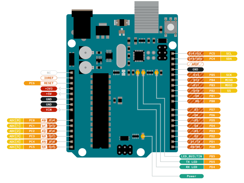
Arduino UNO PinOut and PinMux
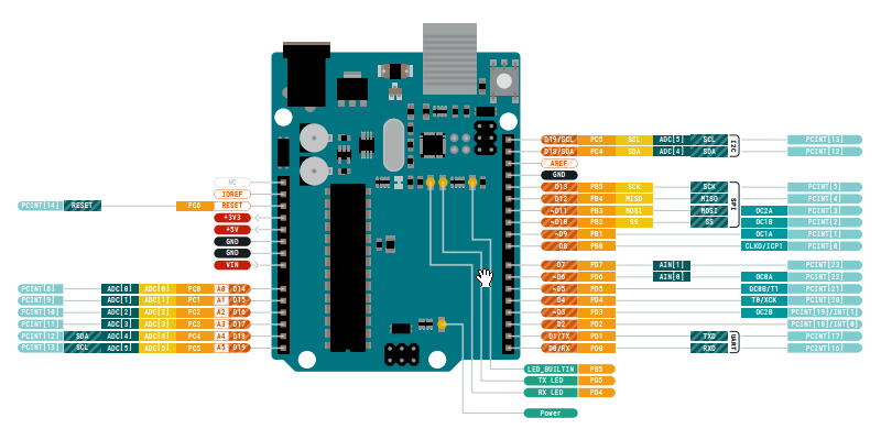
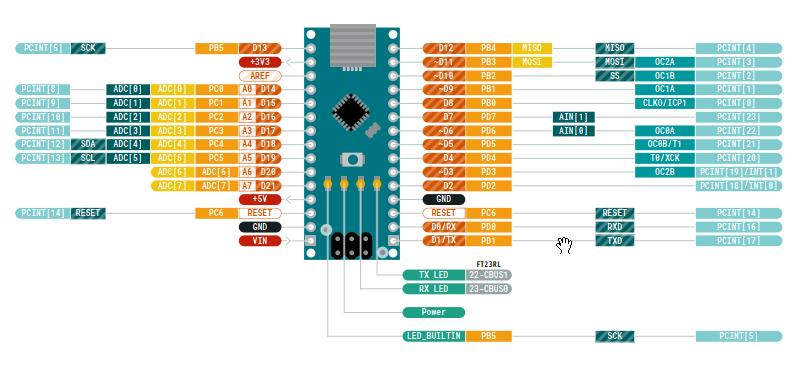
| Atmega328P Chip | Arduino UNO Pin Name | Arduino Description | Alternative Functions |
| PD0 | RX / D0 | Digital IO Pin 0 | Serial RX Pin |
| PD1 | TX / D1 | Digital IO Pin 1 | Serial TX Pin |
| PD2 | D2 | Digital IO Pin 2 | INT0 |
| PD3 | D3 | Digital IO Pin 3 | Timer (OC2B) / INT1 |
| PD4 | D4 | Digital IO Pin 4 | Timer (T0/XCK) |
| PD5 | D5 | Digital IO Pin 5 | Timer (OC0B/T1) |
| PD6 | D6 | Digital IO Pin 6 | Timer (OC0A) / AIN0 |
| PD7 | D7 | Digital IO Pin 7 | AIN1 |
| PB0 | D8 | Digital IO Pin 8 | Timer (CLK0/ICP1) |
| PB1 | D9 | Digital IO Pin 9 | Timer (OC1A) |
| PB2 | D10 | Digital IO Pin 10 | Timer (OC1B) |
| PB3 | D11 | Digital IO Pin 11 | SPI (MOSI) Timer (OC2A) |
| PB4 | D12 | Digital IO Pin 12 | SPI (MISO) |
| PB5 | D13 | Digital IO Pin 13 | SPI (SCK) |
| GND | GND | Power Ground | |
| AREF | AREF | Analog Reference | |
| PC4 | SDA / D18 | Digital IO Pin 18 | I2C Data Pin / ADC4 |
| PC5 | SCL / D19 | Digital IO Pin 19 | I2C Clock Pin / ADC5 |
| – | – | Not Connected | |
| VCC | IOREF | Voltage Reference (VCC) | |
| PC6 | RESET | Reset (Active LOW) | Digital IO Pin |
| – | 3V3 | Power | |
| VCC | 5V | +5V Output from regulator or +5V regulated Input | |
| GND | GND | Ground | |
| GND | GND | Ground | |
| – | VIN | Unregulated Supply | |
| PC0 | A0 / D14 | Analog Input 0 | Digital IO Pin 14 |
| PC1 | A1 / D15 | Analog Input 1 | Digital IO Pin 15 |
| PC2 | A2 / D16 | Analog Input 2 | Digital IO Pin 16 |
| PC3 | A3 / D17 | Analog Input 3 | Digital IO Pin 17 |
| PC4 | A4 / D18 | Analog Input 4 | Digital IO Pin 18 / I2C (SDA) |
| PC5 | A5 / D19 | Analog Input 5 | Digital IO Pin 19 / I2C (SCL) |
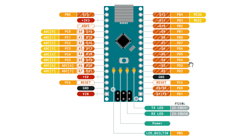
| A6 / D20 | Analog Input 6 | Only Arduino NANO | |
| A7 / D21 | Analog Input 7 | Only Arduino NANO |
Arduino NANO PinOut and PinMux

0 Comments