Note
This article is a part of Arduino / ATmega328p Embedded C Firmware Programming Tutorial. Consider exploring the course home page for articles on similar topics.

Arduino Tutorial Embedded C Register Level Arduino Master Class
Also visit the Release Page for Register Level Embedded C Hardware Abstraction Library and Code for AVR.
Introduction
The Serial Peripheral Interface (SPI) is a full duplex synchronous serial communication interface specification used for short-distance communication, primarily in embedded systems. The interface was developed by Motorola in the mid-1980s. The SPI communication is a master – slave protocol with a single master device and one or more slave devices. Serial Peripheral Interface (SPI) is used for communicating with microcontrollers, microprocessors, LCDs, SD Cards, sensors (Gyroscope etc.), memory devices (Flash, EEPROM) and is widely used in modern day embedded hardwares.
SPI protocol was invented for replacing Parallel Bus Communication that was most prevalent during 90s. Parallel bus communication required at least 10 pins / wires for 8 bit data transfer whereas SPI used only 4.
What You Will Learn
- How does SPI communication work in Arduino?
- How does SPI communication work in AVR ATmega328p?
- What are the Pros and Cons of SPI communication?
- What is the SPI Data Frame format?
SPI Features
- Full duplex communication
- Single master – multi slave architecture
- High speed communication [Hz, kHz or MHz]
- Push-Pull hardware pin drivers
- Four wire / pin serial bus
- MOSI / Master Out Slave In – Output data from the master device to the input of the slave device
- MISO / Master In Slave Out – Output data from a slave device to the input of the master device
- SCLK / Serial Clock – Clock driven by the master device to slave device, used to synchronize the data bits
- SS / Slave Select – Select signal (active low) driven by the master device to individual slave devices, used to select the target slave (also called CE / CS)
- Flexible protocol – no constrains on data length, framing, addressing
- Short distance communication, usually on the same PCB / system
| Term | Description |
|---|---|
| Master | The device that initiates and terminates a transmission. The master also generates the SCLK clock |
| Slave | The device selected by a master |
| Transmitter | The device placing data on the bus |
| Receiver | The device reading data from the bus |
SPI Bus Protocol
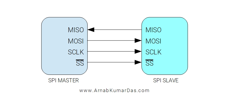
SPI bus uses four wires / pins to communicate between two devices. The four wires / pins are MOSI, MISO, SCLK and SS. Data flows in and out through the MISO and MOSI pins. The SCLK pin is used to synchronize the data transfer by supplying a clock signal. The SS is used to select the slave device with which the master device wants to communicate. In other words SS / CE is used to initiate and terminate the data transfer. The SS pin is active low which means the slave device responds only when the logic on the pin goes LOW.
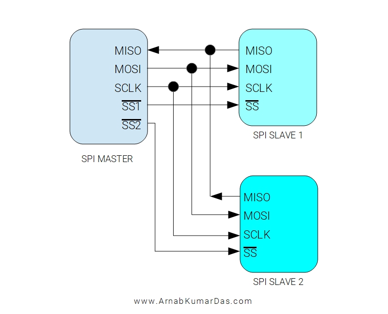
In multi slave mode the MISO, MOSI and SCLK are shared whereas independent SS pins are used for each slave device. Multi slave communication is only possible when all the slave’s MISO pin is tri-state buffered. Master communicates with one slave at a time by selecting respective SS pin.
Some of the important components of the SPI hardware are the clock generator, shift register, data buffer and pin control logic.
To begin any communication the first step is to configure the clock generator of the master device to generate a clock pulse on the SCLK pin of a frequency that the slave supports.
SPI consists of two shift register, one in the master device and the other in the slave device. Serial-out of the master shift register is connected to serial-in of slave shift register via MOSI pin. Serial-out of the slave shift register is connected to serial-in of master shift register via MISO pin. On a clock edge, both master and slave shifts out 1 bit data ( most significant bit (MSB) ) from their respective shift registers on the transmission line . On the next clock edge, at each receiver the bit is sampled from the transmission line and set as a new least-significant bit of the respective shift register.
For some slaves, LSB is transmitted first. Some microcontrollers allows to configure this through the SPI configuration registers.
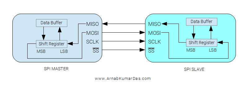
The shift registers are loaded from the data buffer, before start of a transmission and also unloaded to the data buffer after end of the reception. Transmission may continue for any number of clock cycles. When complete, the master stops toggling the clock signal, and typically deselects the slave.
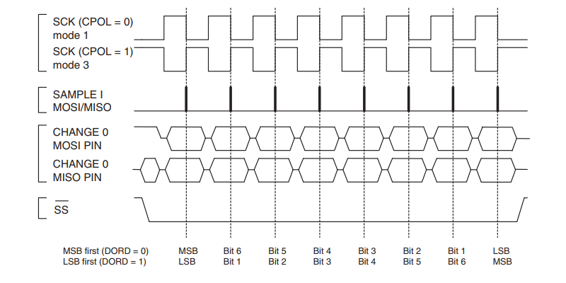
SPI Clock Polarity and Phase
In addition to configuring the clock to a set the frequency, the master should also configure the clock polarity and phase. Clock polarity is called CPOL and clock phase is called CPHA. Usually CPOL and CPHA are bits in the SPI configuration register and can take either 0 (LOW) or 1 (HIGH) as value. Based on the CPOL and CPHA configuration the data on the bus is written and sampled with respect to the clock signal. CPOL and CPHA configuration should be same for both master and slave.
| CPOL | Leading Edge | Trailing Edge |
|---|---|---|
| 0 | Rising | Falling |
| 1 | Falling | Rising |
When this bit is written to one, SCLK is HIGH when idle. When CPOL is written to zero, SCLK is LOW when idle.
| CPHA | Leading Edge | Trailing Edge |
|---|---|---|
| 0 | Data Sample | Data Setup / Change |
| 1 | Data Setup / Change | Data Sample |
The settings of the Clock Phase bit (CPHA) determine if data is sampled on the leading (first) or trailing (last) edge of SCLK.
Mode 0 : CPOL=0, CPHA=0. When SPI is idle, the clock output is logic LOW; data changes on the falling edge of the SPI clock and is sampled on the rising edge.
Mode 1 : CPOL=0, CPHA=1. When SPI is idle, the clock output is logic LOW; data changes on the rising edge of the SPI clock and is sampled on the falling edge.
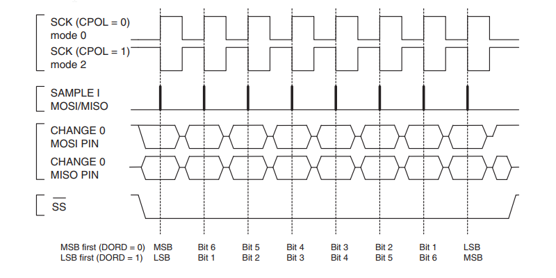
Mode 2 : CPOL=1, CPHA=0. When SPI is idle, the clock output is logic HIGH; data changes on the rising edge of the SPI clock and is sampled on the falling edge.
Mode 3 : CPOL=1, CPHA=1. When SPI is idle, the clock output is logic HIGH; data changes on the falling edge of the SPI clock and is sampled on the rising edge.
SPI Read and Write
- Single Byte Write
- Multibyte Burst Write
- Single Byte Write
- Multibyte Burst Write
Single Byte Write
- Make CE = 0 to select slave
- Load the 1 byte of data in the SPI shift register
- Wait till transmission is complete
- Make CE = 1 to deselect slave
Multibyte Burst Write
- Make CE = 0 to select slave
- Load the 1 byte of data in the SPI shift register
- Wait till transmission is complete
- Repeat step 2 and 3 till all bytes are transferred
- Make CE = 1 to deselect slave
Single Byte Read
- Make CE = 0 to select slave
- Wait till transmission is complete
- Read the 1 byte of received data from the SPI shift register
- Make CE = 1 to deselect slave
Multibyte Burst Read
- Make CE = 0 to select slave
- Wait till transmission is complete
- Read the 1 byte of received data from the SPI shift register
- Repeat step 2 and 3 till all bytes are received
- Make CE = 1 to deselect slave
Advantages
- Full duplex communication
- High throughput
- Push pull driver provides better signal integrity
- No data frame length limit
- Uses 4 wires
- Transceivers are not needed
- Galvanic isolation possible
- Simple software implementation
Disadvantages
- Slaves should have tri-state buffer for MISO pin so that they can disconnect the line when the Master has not selected the device. This is necessary for multi slave communication
- No hardware flow control
- No hardware slave acknowledgement
- No hardware error checking
- Short distance communiaction
- Single master protocol

2 Comments
MG_FF · September 20, 2021 at 6:42 am
You said you introduced the data frame format, but you didn’t.
Crazy Engineer · September 20, 2021 at 9:51 am
You have to read through the tutorial. The topic is discussed.