Note
This article is a part of Arduino / ATmega328p Embedded C Firmware Programming Tutorial. Consider exploring the course home page for articles on similar topics.

Arduino Tutorial Embedded C Register Level Arduino Master Class
Also visit the Release Page for Register Level Embedded C Hardware Abstraction Library and Code for AVR.
Introduction
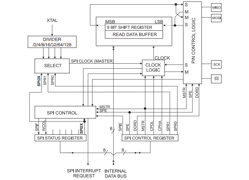
The Serial Peripheral Interface (SPI) hardware in the ATmega48A/PA/88A/PA/168A/PA/328/P microcontroller uses three registers SPCR, SPSR and SPDR to configure the hardware and to transmit and receive data. Below are the register descriptions.
What You Will Learn
- What are the SPI Registers in Arduino?
- What are the SPI Registers in AVR ATmega328p?
- Which AVR Registers control and configures Serial Peripheral Interface?
- What is the function of the SPI Registers?
SPCR – SPI Control Register
| Bit | 7 | 6 | 5 | 4 | 3 | 2 | 1 | 0 |
| 0x2C (0x4C) | SPIE | SPE | DORD | MSTR | CPOL | CPHA | SPR1 | SPR0 |
| Read/Write | R/W | R/W | R/W | R/W | R/W | R/W | R/W | R/W |
| Initial Value | 0 | 0 | 0 | 0 | 0 | 0 | 0 | 0 |
• Bit 7 – SPIE: SPI Interrupt Enable
This bit causes the SPI interrupt to be executed if SPIF bit in the SPSR Register is set and the if the Global Interrupt Enable bit in SREG is set.
• Bit 6 – SPE: SPI Enable
When the SPE bit is written to one, the SPI is enabled. This bit must be set to enable any SPI operations.
• Bit 5 – DORD: Data Order
When the DORD bit is written to one, the LSB of the data word is transmitted first. When the DORD bit is written to zero, the MSB of the data word is transmitted first.
• Bit 4 – MSTR: Master/Slave Select
This bit selects Master SPI mode when written to one, and Slave SPI mode when written logic zero. If SS is configured as an input and is driven low while MSTR is set, MSTR will be cleared, and SPIF in SPSR will become set. The user will then have to set MSTR to re-enable SPI Master mode.
• Bit 3 – CPOL: Clock Polarity
When this bit is written to one, SCK is high when idle. When CPOL is written to zero, SCK is low when idle. The CPOL functionality is summarized below:
| CPOL | Leading Edge | Trailing Edge |
| 0 | Rising | Falling |
| 1 | Falling | Rising |
• Bit 2 – CPHA: Clock Phase
The settings of the Clock Phase bit (CPHA) determine if data is sampled on the leading (first) or trailing (last) edge of SCK. The CPOL functionality is summarized below:
| CPHA | Leading Edge | Trailing Edge |
| 0 | Sample | Setup |
| 1 | Setup | Sample |
• Bits 1, 0 – SPR1, SPR0: SPI Clock Rate Select 1 and 0
These two bits control the SCK rate of the device configured as a Master. SPR1 and SPR0 have no effect on the Slave. The relationship between SCK and the Oscillator Clock frequency fosc is shown in the following table:
| SPI2X | SPR1 | SPR0 | SCK Frequency |
| 0 | 0 | 0 | fosc/4 |
| 0 | 0 | 1 | fosc/16 |
| 0 | 1 | 0 | fosc/64 |
| 0 | 1 | 1 | fosc/128 |
| 1 | 0 | 0 | fosc/2 |
| 1 | 0 | 1 | fosc/8 |
| 1 | 1 | 0 | fosc/32 |
| 1 | 1 | 1 | fosc/64 |
SPSR – SPI Status Register
| Bit | 7 | 6 | 5 | 4 | 3 | 2 | 1 | 0 |
| 0x2D (0x4D) | SPIF | WCOL | – | – | – | – | – | SPI2X |
| Read/Write | R | R | R | R | R | R | R | R |
| Initial Value | 0 | 0 | 0 | 0 | 0 | 0 | 0 | 0 |
• Bit 7 – SPIF: SPI Interrupt Flag
When a serial transfer is complete, the SPIF Flag is set. An interrupt is generated if SPIE in SPCR is set and global interrupts are enabled. If SS is an input and is driven low when the SPI is in Master mode, this will also set the SPIF Flag. SPIF is cleared by hardware when executing the corresponding interrupt handling vector. Alternatively, the SPIF bit is cleared by first reading the SPI Status Register with SPIF set, then accessing the SPI Data Register (SPDR).
• Bit 6 – WCOL: Write COLlision Flag
The WCOL bit is set if the SPI Data Register (SPDR) is written during a data transfer. The WCOL bit (and the SPIF bit) are cleared by first reading the SPI Status Register with WCOL set, and then accessing the SPI Data Register.
• Bit [5:1] – Reserved
These bits are reserved bits in the ATmega48A/PA/88A/PA/168A/PA/328/P and will always read as zero.
• Bit 0 – SPI2X: Double SPI Speed Bit
When this bit is written logic one the SPI speed (SCK Frequency) will be doubled when the SPI is in Master mode. This means that the minimum SCK period will be two CPU clock periods. When the SPI is configured as Slave, the SPI is only guaranteed to work at fosc/4 or lower.
SPDR – SPI Data Register
| Bit | 7 | 6 | 5 | 4 | 3 | 2 | 1 | 0 |
| 0x2E (0x4E) | MSB | LSB | ||||||
| Read/Write | R/W | R/W | R/W | R/W | R/W | R/W | R/W | R/W |
| Initial Value | X | X | X | X | X | X | X | X |
The SPI Data Register is a read/write register used for data transfer between the Register File and the SPI Shift Register. Writing to the register initiates data transmission. Reading the register causes the Shift Register Receive buffer to be read.


0 Comments