Note
This article is a part of Arduino / ATmega328p Embedded C Firmware Programming Tutorial. Consider exploring the course home page for articles on similar topics.

Arduino Tutorial Embedded C Register Level Arduino Master Class
Also visit the Release Page for Register Level Embedded C Hardware Abstraction Library and Code for AVR.
Introduction
This section discusses the AVR architecture in general. There are other articles in this series that discuss AVR architecture in detail.
In this article, we will be discussing the overview of AVR CPU Core, Registers, Memories, Interfaces, Clock, etc.
What You Will Learn
- What are the different components in Arduino CPU?
- What are the different components in AVR ATmega328p CPU?
- What are the Memory and Programming Interfaces in AVR ATmega328p?
AVR 8-bit CPU Core Block
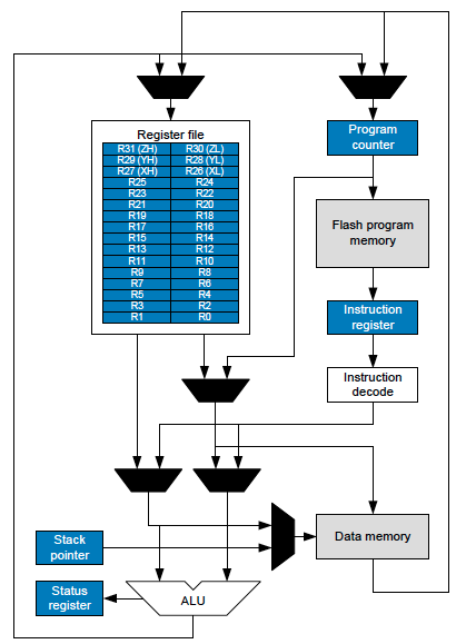
The AVR uses a Harvard architecture with separate memories and buses for program and data. Instructions in the program memory are executed with a single level pipelining and are classified as 8-bit RISC devices. While one instruction is being executed, the next instruction is pre-fetched from the program memory. This concept enables instructions to be executed in every clock cycle. Flash, EEPROM, and SRAM are all integrated into a single chip in AVR microcontrollers. The Data Bus is 8-bit in width.
AVR Registers
AVR contains 32 x 8-bit general purpose working registers with a single clock cycle access time. Six of the 32 registers can be used as three 16-bit indirect address register pointers (X-, Y-, and Z-registers) for Data Space addressing. One of these address pointers can also be used as an address pointer for look-up tables in Flash program memory.
The 32 x 8-bit general purpose working registers are mapped into the first 32 memory addresses (000016–001F16), followed by 64 I/O registers (002016–005F16).
AVR Arithmetic Logic Unit (ALU)
The ALU supports arithmetic and logic operations between registers or between a constant and a register. Single clock cycle access of 32 x 8-bit general purpose working register allows single-cycle ALU operations.
In a general ALU computation, two registers are used as operands, the operation is executed and the result is stored back in a register in one clock cycle. Single register operations can also be executed in the ALU. After an arithmetic computation, the Status register is updated to indicate information about the result of the operation.
The ALU operations are divided into three main categories – arithmetic, logical, and bit functions. Some implementations of the architecture also provide a powerful multiplier supporting both signed/unsigned multiplication and fractional format.
Program Flash Memory
The memory spaces in the AVR architecture are designed in a linear and regular memory map. The size of the flash program memory is usually indicated in the part number of the device itself (e.g., the ATmega32x line has 32KB of flash, while the ATmega64x line has 64KB). The AVR Flash is an on-chip in-system reprogrammable flash memory for program instruction storage. The Flash memory has a typical endurance of at least 10,000 writes/erase cycles
AVR Program Flash memory space is divided into two sections, the Boot Program section and the Application Program section. Lock bits are available to read/write protection to prevent tampering. The application section can be updated by the bootloader.
Since all AVR instructions are 16 or 32-bits wide the flash is arranged in 16-bit width word size.
Data Memory
AVR Data Memory is implemented in a separate address bus than the Program Memory. There are two data buses, one that can access all data and the In/Out data bus with limited access to a small section of memory.
The AVR Data Address Space consists of :
- Registers (32 x 8-bit) (000016–001F16)
Consists of 32 8-bit general purpose working registers (R0-R31) - I/O Memory (64 x 8-bit) (002016–005F16)
Contains addressable space for peripheral control registers and other I/O registers - Extended I/O Memory (device dependent) (160 x 8-bit) (006016–00FF16)
Some AVR microcontrollers with more peripherals need more space than the I/O memory can address so some of the SRAM is used as Extended I/O memory to handle the extra peripherals control registers and other I/O functions - Internal SRAM (2048 x 8-bit) (010016–08FF16)
SRAM is used for temporarily storing intermediate results and variables, stack within a software application.
EEPROM
AVR Electrically Erasable Programmable Read-Only Memory (EEPROM) is organized as a separate data space, in which single bytes can be read and written. The EEPROM has an endurance of at least 100,000 writes/erase cycles. Erase and write can be performed separately in many cases, byte-by-byte, which may also help prolong life when bits only need to be set to all 1s (erase) or selectively cleared to 0s (write).
Access from the CPU to EEPROM is done through the EEPROM Address Registers, the EEPROM Data Register, and the EEPROM Control Register.
MCU Clock Speed and MIPS Performance
Most AVR devices support 1MHz to 20MHz Clock Speed. AVR also has an internal oscillator removing the need for external clocks or resonator circuitry. Some AVRs also have a system clock Prescaler that can divide down the system clock by up to 1024. This Prescaler can be reconfigured by software during run-time, allowing the clock speed to be changed on the go.
AVR can achieve up to 1 MIPS per MHz, i.e. a 12 MHz processor can achieve up to 12 MIPS. Most instructions take one clock cycle to execute. Loads and stores to/from memory take two cycles, branching takes two cycles.
Programming Interfaces
AVR microcontrollers support multiple ways of programming/loading program code to the chip. The methods to program AVR chips vary from AVR family to family. Most of the methods described below use the RESET line to enter programming mode.
ISP (In-System Programming)
In-system programming is performed through the SPI interface. It Involves 6 pins for the connection MISO, MOSI, SCK, RST, VCC, and GND. ISP works even when the chip is soldered to the PCB and the SPI signals are not disturbed. ISP programming is supported by the official Atmel-ICE tool and many other DIY and open-source tools. It is not a debugging interface. It can be used to download code into the flash and EEPROM
PDI (Program and Debug Interface)
The Program and Debug Interface is an Atmel proprietary interface for external programming and on-chip debugging of XMEGA devices. PDI used the NVM controller to flash and debug software serially. The PDI is a 2-pin interface using the Reset pin for clock input (PDI_CLK) and a dedicated data pin (PDI_DATA) for input and output. PDI is a 2-pin interface providing a bi-directional half-duplex synchronous communication with the target device.
UPDI (Unified Program and Debug Interface)
Unified Program and Debug Interface is a proprietary interface for external programming and on-chip debugging of a device. It is a successor to the PDI 2-wire physical interface, UPDI is a single-wire interface providing a bi-directional half-duplex asynchronous communication with the target device for purposes of programming and debugging.
HVSP (High Voltage Serial Programming)
High Voltage Serial Programming can be used to program AVR microcontrollers as a backup programming method when ISP is not available. Usually, HVSP is used for 8- and 14-pin ATtiny microcontrollers. It uses multiple pins but the most important one is a 12V signal to be applied to the RESET pin of the target microcontroller.
HVPP (High Voltage Parallel Programming)
High Voltage Parallel Programming is used as a backup option to revive locked chips or to correct bad fuse settings in AVR microcontrollers. This also uses a 12V signal to RESET pin of the target microcontroller. HVPP is the high voltage protocol for ATtiny and ATmega MCUs with 20 pins or more.
JTAG (Joint Test Action Group)
JTAG provides access to on-chip debugging functionality while the chip is running in the target system. JTAG allows access to internal memory and registers, setting breakpoints on code, and single-stepping execution to observe system behavior.
debugWIRE
debugWIRE provides on-chip debug capabilities via a single microcontroller pin. The debugWIRE interface can not be used as a programming interface. This means that the SPI interface connection must also be available in order to program the target via ISP.
Conclusion
In this article, we overall discussed some core components of the AVR architecture. In the next articles, we will be discussing the core architecture in detail.

3 Comments
Gopinath · August 23, 2022 at 2:00 am
Really useful information and I hope it will be helpful for my development futures.
Anon · September 26, 2022 at 6:48 pm
Article is densely packed with information without any intuitive connection between them. Someone coming to gain new knowledge won’t consolidate anything new in their head, and anyone already experienced in this tech would not read the article anyways as it would be redundant to them.
gbalcita · December 29, 2022 at 7:50 pm
Great article. I have been playing around with Arduino for a few years now and looking to get into general purpose microcontrollers. I know this info is probably in the datasheets but I have read datasheets extensively for atmega328p and attiny84 and I do not ever recall the high voltage programming stuff (but I was not specifically looking for them). Thanks for the post.