Note
This article is a part of Arduino / ATmega328p Embedded C Firmware Programming Tutorial. Consider exploring the course home page for articles on similar topics.

Arduino Tutorial Embedded C Register Level Arduino Master Class
Also visit the Release Page for Register Level Embedded C Hardware Abstraction Library and Code for AVR.
Introduction
This section discusses the AVR CPU Core, ALU, Status Register, Stack Pointer, Interrupt handling, and Instruction processing. The main function of the CPU core is to ensure correct program execution. The AVR CPU is capable to access memories, perform calculations, control peripherals, and handle interrupts. The components of the CPU were discussed in the AVR Architecture article.
What You Will Learn
- How the Arduino CPU works?
- How the CPU of AVR ATmega328p chip works?
- What are the CPU components of ATmega328p?
- What are the different CPU instructions in ATmega328p?
- How many CPU Registers are there in Arduino/ATmega328p?
8-Bit AVR CPU Operation
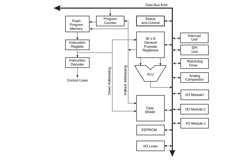
AVR uses a Harvard architecture – with separate memories and buses for program and data. Instructions in the program memory are executed with a single level pipelining. This improves performance and parallelism. While one instruction is being executed, the next instruction is pre-fetched from the program memory. This concept enables instructions to be executed in every clock cycle. The program memory is In-System Reprogrammable Flash memory.
The fast-access Register File contains 32 x 8-bit general purpose working registers with a single clock cycle access time. This allows single-cycle Arithmetic Logic Unit (ALU) operation. In a typical ALU operation, two operands are output from the Register File, the operation is executed, and the result is stored back in the Register File in one clock cycle.
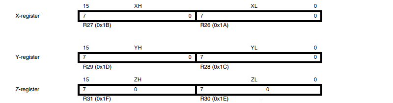
Six of the 32 registers can be used as three 16-bit indirect address register pointers for Data Space addressing – enabling efficient address calculations. One of these address pointers can also be used as an address pointer for look up tables in Flash program memory. These added function registers are the 16-bit X-, Y-, and Z register described later in this section.
The ALU supports arithmetic and logic operations between registers or between a constant and a register. Single register operations can also be executed in the ALU. After an arithmetic operation, the Status Register is updated to reflect information about the result of the operation.
Program flow is provided by conditional and unconditional jump and call instructions, able to directly address the whole address space. Most AVR instructions have a single 16-bit word format. Every program memory address contains a 16- or 32-bit instruction.
Program Flash memory space is divided into two sections, the Boot Program section and the Application Program section. Both sections have dedicated Lock bits for write and read/write protection. The SPM instruction writes into the Application Flash memory section must reside in the Boot Program section. During interrupts and subroutine calls, the return address Program Counter (PC) is stored on the Stack. The Stack is effectively allocated in the general data SRAM, and consequently, the Stack size is only limited by the total SRAM size and the usage of the SRAM. All user programs must initialize the SP in the Reset routine (before subroutines or interrupts are executed). The Stack Pointer (SP) is read/write accessible in the I/O space. The data SRAM can easily be accessed through the five different addressing modes supported in the AVR architecture.
The memory spaces in the AVR architecture are all linear and regular memory maps. A flexible interrupt module has its control registers in the I/O space with an additional Global Interrupt Enable bit in the Status Register. All interrupts have a separate Interrupt Vector in the Interrupt Vector table. The interrupts have priority in accordance with their Interrupt Vector position. The lower the Interrupt Vector address, the higher the priority.
8-Bit AVR Arithmetic Logic Unit (ALU)
The high-performance AVR ALU operates in direct connection with all the 32 general purpose working registers. Within a single clock cycle, arithmetic operations between general purpose registers or between a register and an immediate are executed. The ALU operations are divided into three main categories – arithmetic, logical, and bit functions.
| Mnemonics | Operands | Description | Operation | Flags | Clock |
|---|---|---|---|---|---|
| ADD | Rd, Rr | Add two Registers | Rd <- Rd + Rr | Z,C,N,V,H | 1 |
| ADC | Rd, Rr | Add with Carry two Registers | Rd <- Rd + Rr + C | Z,C,N,V,H | 1 |
| ADIW | Rdl,K | Add Immediate to Word | Rdh:Rdl <- Rdh:Rdl + K | Z,C,N,V,S | 2 |
| SUB | Rd, Rr | Subtract two Registers | Rd <- Rd – Rr | Z,C,N,V,H | 1 |
| SUBI | Rd, K | Subtract Constant from Register | Rd <- Rd – K | Z,C,N,V,H | 1 |
| SBC | Rd, Rr | Subtract with Carry two Registers | Rd <- Rd – Rr – C | Z,C,N,V,H | 1 |
| SBCI | Rd, K | Subtract with Carry Constant from Reg. | Rd <- Rd – K – C | Z,C,N,V,H | 1 |
| SBIW | Rdl,K | Subtract Immediate from Word | Rdh:Rdl <- Rdh:Rdl – K | Z,C,N,V,S | 2 |
| AND | Rd, Rr | Logical AND Registers | Rd <- Rd & Rr | Z,N,V | 1 |
| ANDI | Rd, K | Logical AND Register and Constant | Rd <- Rd & K | Z,N,V | 1 |
| OR | Rd, Rr | Logical OR Registers | Rd <- Rd | Rr | Z,N,V | 1 |
| ORI | Rd, K | Logical OR Register and Constant | Rd <- Rd | K | Z,N,V | 1 |
| EOR | Rd, Rr | Exclusive OR Registers | Rd <- Rd ⊕ Rr | Z,N,V | 1 |
| COM | Rd | One’s Complement | Rd <- 0xFF – Rd | Z,C,N,V | 1 |
| NEG | Rd | Two’s Complement | Rd <- 0x00 – Rd | Z,C,N,V,H | 1 |
| SBR | Rd,K | Set Bit(s) in Register | Rd <- Rd | K | Z,N,V | 1 |
| CBR | Rd,K | Clear Bit(s) in Register | Rd <- Rd & (0xFF – K) | Z,N,V | 1 |
| INC | Rd | Increment | Rd <- Rd + 1 | Z,N,V | 1 |
| DEC | Rd | Decrement | Rd <- Rd – 1 | Z,N,V | 1 |
| TST | Rd | Test for Zero or Minus | Rd <- Rd & Rd | Z,N,V | 1 |
| CLR | Rd | Clear Register | Rd <- Rd ⊕ Rd | Z,N,V | 1 |
| SER | Rd | Set Register | Rd <- 0xFF | None | 1 |
| MUL | Rd, Rr | Multiply Unsigned | R1:R0 <- Rd x Rr | Z,C | 2 |
| MULS | Rd, Rr | Multiply Signed | R1:R0 <- Rd x Rr | Z,C | 2 |
| MULSU | Rd, Rr | Multiply Signed with Unsigned | R1:R0 <- Rd x Rr | Z,C | 2 |
| FMUL | Rd, Rr | Fractional Multiply Unsigned | R1:R0 <- (Rd x Rr) << 1 | Z,C | 2 |
| FMULS | Rd, Rr | Fractional Multiply Signed | R1:R0 <- (Rd x Rr) << 1 | Z,C | 2 |
| FMULSU | Rd, Rr | Fractional Multiply Signed with Unsigned | R1:R0 <- (Rd x Rr) << 1 | Z,C | 2 |
| Mnemonics | Operands | Description | Operation | Flags | Clocks |
8-Bit AVR Status Register
The Status Register contains information about the result of the most recently executed arithmetic instruction. This information can be used for altering program flow in order to perform conditional operations. Status Register is updated after all ALU operations. This will in many cases remove the need for using the dedicated compare instructions, resulting in faster and more compact code.
The Status Register is not automatically stored when entering an interrupt routine and restored when returning from an interrupt. This must be handled by software. When addressing I/O Registers as data space using LD and ST instructions, the provided offset must be used. When using the I/O specific commands IN and OUT, the offset is reduced by 0x20, resulting in an I/O address offset within 0x00-0x3F.
| Bit | 7 | 6 | 5 | 4 | 3 | 2 | 1 | 0 |
| Read/Write Initial Value | R/W 0 | R/W 0 | R/W 0 | R/W 0 | R/W 0 | R/W 0 | R/W 0 | R/W 0 |
| SREG 0x3F (0x5F) | I | T | H | S | V | N | Z | C |
• Bit 7 – I: Global Interrupt Enable
The Global Interrupt Enable bit must be set for the interrupts to be enabled. The individual interrupt enable control is then performed in separate control registers. If the Global Interrupt Enable Register is cleared, none of the interrupts is enabled independent of the individual interrupt enable settings.
• Bit 6 – T: Bit Copy Storage
The Bit Copy instructions BLD (Bit LoaD) and BST (Bit STore) use the T-bit as source or destination for the operated bit.
• Bit 5 – H: Half Carry Flag
The Half Carry Flag H indicates a Half Carry in some arithmetic operations. Half Carry Is useful in BCD arithmetic.
• Bit 4 – S: Sign Bit, S = N⊕ V
The S-bit is always an exclusive or between the Negative Flag N and the Two’s Complement Overflow Flag V.
• Bit 3 – V: Two’s Complement Overflow Flag
The Two’s Complement Overflow Flag V supports two’s complement arithmetic.
• Bit 2 – N: Negative Flag
The Negative Flag N indicates a negative result in an arithmetic or logic operation.
• Bit 1 – Z: Zero Flag
The Zero Flag Z indicates a zero result in an arithmetic or logic operation.
• Bit 0 – C: Carry Flag
The Carry Flag C indicates a carry in an arithmetic or logic operation.
8-Bit AVR General Purpose Registers
The Register File is optimized for the AVR Enhanced RISC instruction set. In order to achieve the required performance and flexibility, the following input/output schemes are supported by the Register File:
- One 8-bit output operand and one 8-bit result input
- Two 8-bit output operands and one 8-bit result input
- Two 8-bit output operands and one 16-bit result input
- One 16-bit output operand and one 16-bit result input
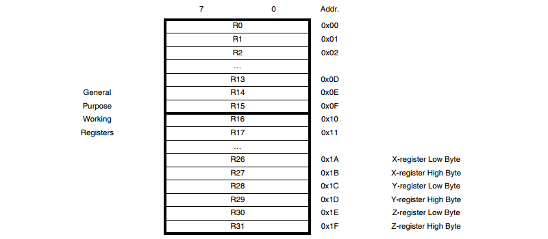
Most of the instructions operating on the Register File have direct access to all registers, and most of them are single cycle instructions. Each register is also assigned a data memory address, mapping them directly into the first 32 locations of the user Data Space. Although not being physically implemented as SRAM locations, this memory organization provides great flexibility in access of the registers, as the X-, Y- and Z-pointer registers can be set to index any register in the file.
The registers R26…R31 have some added functions to their general purpose usage. These registers are 16-bit address pointers for indirect addressing of the data space.
8-Bit AVR Stack Pointer / Register
The stack is mainly used for storing temporary data, local variables, and return addresses after interrupts and subroutine calls. It is implemented as growing from higher to lower memory locations. The Stack Pointer Register always points to the top of the stack; it points to the data SRAM Stack area where the subroutine and interrupt stacks are located.
The Stack in the data SRAM must be defined by the program before any subroutine calls are executed or interrupt are enabled. Initial Stack Pointer value equals the last address of the internal SRAM and the Stack Pointer must be set to point above the start of the SRAM. The AVR Stack Pointer is implemented as two 8-bit registers in the I/O space. The number of bits actually used depends on the implementation. Data space in some implementations of the AVR architecture is so small that only the Stack Pointer Low (SPL) register is needed. In this case, the Stack Pointer High (SPH) register will not be present.
| Bit | 15 | 14 | 13 | 12 | 11 | 10 | 9 | 8 |
| 0x3E (0x5E) | SP15 | SP14 | SP13 | SP12 | SP11 | SP10 | SP9 | SP8 |
| 0x3D (0x5D) | SP7 | SP6 | SP5 | SP4 | SP3 | SP2 | SP1 | SP0 |
| Read/Write | 7 R/W R/W | 6 R/W R/W | 5 R/W R/W | 4 R/W R/W | 3 R/W R/W | 2 R/W R/W | 1 R/W R/W | 0 R/W R/W |
| Initial Value | RAMEND RAMEND | RAMEND RAMEND | RAMEND RAMEND | RAMEND RAMEND | RAMEND RAMEND | RAMEND RAMEND | RAMEND RAMEND | RAMEND RAMEND |
| Instruction | Stack pointer | Description |
|---|---|---|
| PUSH | Decrement by 1 | Data is pushed onto the stack |
| CALL ICALL RCALL | Decrement by 2 | The return address is pushed onto the stack with a subroutine call or interrupt |
| POP | Increment by 1 | Data is popped from the stack |
| RET RETI | Increment by 2 | The return address is popped from the stack with return from subroutine or return from interrupt |
8-Bit AVR Instruction Execution Timing
The AVR CPU is driven by the CPU clock clkCPU, directly generated from the selected clock source for the chip. No internal clock division is used. The basic pipelining concept is used to obtain up to 1 MIPS per MHz. The parallel instruction fetches and instruction executions enabled by the Harvard architecture and the fast-access Register File enable this performance.
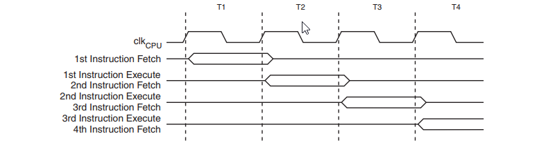
In a single clock cycle, an ALU operation using two register operands is executed, and the result is stored back to the destination register.

8-Bit AVR Reset and Interrupt Handling and Timing
The AVR provides several different interrupt sources. These interrupts and the separate Reset Vector each have a separate program vector in the program memory space. All interrupts are assigned individual enable bits which must be written logic one together with the Global Interrupt Enable bit in the Status Register in order to enable the interrupt.
This list determines the priority levels of the different interrupts. The lower the address the higher is the priority level. The lowest addresses in the program memory space are by default defined as the Reset and Interrupt Vectors.
| Vector No. | Program Address | Source | Interrupt Definition |
|---|---|---|---|
| 1 | 0x0000 | RESET | External Pin, Power-on Reset, Brown-out Reset, and Watchdog System Reset |
| 2 | 0x0002 | INT0 | External Interrupt Request 0 |
| 3 | 0x0004 | INT1 | External Interrupt Request 1 |
| 4 | 0x0006 | PCINT0 | Pin Change Interrupt Request 0 |
| 5 | 0x0008 | PCINT1 | Pin Change Interrupt Request 1 |
| 6 | 0x000A | PCINT2 | Pin Change Interrupt Request 2 |
| 7 | 0x000C | WDT | Watchdog Time-out Interrupt |
| 8 | 0x000E | TIMER2 COMPA | Timer/Counter2 Compare Match A |
| 9 | 0x0010 | TIMER2 COMPB | Timer/Counter2 Compare Match B |
| 10 | 0x0012 | TIMER2 OVF | Timer/Counter2 Overflow |
| 11 | 0x0014 | TIMER1 CAPT | Timer/Counter1 Capture Event |
| 12 | 0x0016 | TIMER1 COMPA | Timer/Counter1 Compare Match A |
| 13 | 0x0018 | TIMER1 COMPB | Timer/Coutner1 Compare Match B |
| 14 | 0x001A | TIMER1 OVF | Timer/Counter1 Overflow |
| 15 | 0x001C | TIMER0 COMPA | Timer/Counter0 Compare Match A |
| 16 | 0x001E | TIMER0 COMPB | Timer/Counter0 Compare Match B |
| 17 | 0x0020 | TIMER0 OVF | Timer/Counter0 Overflow |
| 18 | 0x0022 | SPI, STC | SPI Serial Transfer Complete |
| 19 | 0x0024 | USART, RX | USART Rx Complete |
| 20 | 0x0026 | USART, UDRE | USART, Data Register Empty |
| 21 | 0x0028 | USART, TX | USART, Tx Complete |
| 22 | 0x002A | ADC | ADC Conversion Complete |
| 23 | 0x002C | EE READY | EEPROM Ready |
| 24 | 0x002E | ANALOG COMP | Analog Comparator |
| 25 | 0x0030 | TWI | 2-wire Serial Interface |
| 26 | 0x0032 | SPM READY | Store Program Memory Ready |
When an interrupt occurs, the Global Interrupt Enable I-bit is cleared and all interrupts are disabled. The user software can write logic one to the I-bit to enable nested interrupts. All enabled interrupts can then interrupt the current interrupt routine. The I-bit is automatically set when a Return from Interrupt instruction – RETI – is executed. When the AVR exits from an interrupt, it will always return to the main program and execute one more instruction before any pending interrupt is served.
The interrupt execution response for all the enabled AVR interrupts is four clock cycles minimum. After four clock cycles, the program vector address for the actual interrupt handling routine is executed. During this four clock cycle period, the Program Counter is pushed onto the Stack. The vector is normally a jump to the interrupt routine, and this jump takes three clock cycles. If an interrupt occurs during the execution of a multi-cycle instruction, this instruction is completed before the interrupt is served. If an interrupt occurs when the MCU is in sleep mode, the interrupt execution response time is increased by four clock cycles. This increase comes in addition to the start-up time from the selected sleep mode.
A return from an interrupt handling routine takes four clock cycles. During these four clock cycles, the Program Counter (two bytes) is popped back from the Stack, the Stack Pointer is incremented by two, and the I-bit in SREG is set.


0 Comments