ATmega328P ADC Registers
The Registers in One Conversion
Section titled “The Registers in One Conversion”The ADC converts an input voltage to a number from 0 to 1023. The result depends on the selected reference voltage, input channel and result alignment. These registers control the conversion:
| Register | Purpose |
|---|---|
ADMUX |
Reference selection, input channel and result alignment |
ADCSRA |
ADC enable, start, prescaler, interrupt enable and completion flag |
ADCSRB |
Auto-trigger source and comparator input-multiplexer control |
ADCL and ADCH |
The low and high portions of the 10-bit result |
DIDR0 |
Optional disable for digital input buffers on ADC pins |
For a usual Uno setup, REFS0 = 1 selects AVCC as the reference, while REFS1 = 0. AVCC should be connected and decoupled as the board design requires. The input channel number goes in MUX3:0; A0 corresponds to ADC0. Set ADLAR = 0 for a right-adjusted result, which is convenient when using all ten bits.
Choose the ADC Clock
Section titled “Choose the ADC Clock”The ADC clock is the CPU clock divided by a prescaler. With a 16 MHz clock and a divide-by-128 prescaler:
f_ADC = 16 MHz / 128 = 125 kHz
The ATmega328P data sheet recommends an ADC clock in the 50-200 kHz range for maximum resolution. A normal conversion takes 13 ADC clock cycles after the first conversion, which takes longer. At 125 kHz, the nominal steady conversion time is about 13 / 125000 = 104 microseconds. This is a conversion time, not a guarantee that your program can collect samples at exactly that rate.
Start a Conversion and Read It Safely
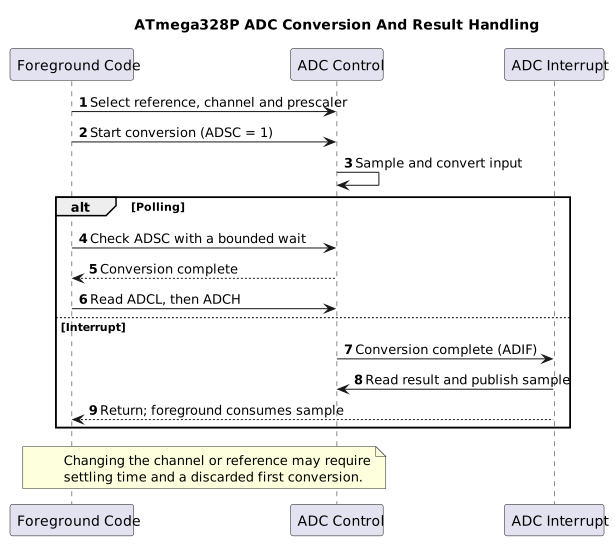
Section titled “Start a Conversion and Read It Safely”The order is reference and channel selection, conversion start, completion check, then low-byte/high-byte result read. The figure in ADC concepts shows the polling and interrupt paths.
This short example shows the register order. It assumes the application owns the ADC and that the ADC clock has already been selected. A production polling function should also have a timeout, so a peripheral fault cannot hold the program forever.
/** * @brief Read ADC0 using AVCC and a right-adjusted result. * @return The ten-bit conversion result in the range 0 to 1023. */static uint16_t adc0_read(void){    uint8_t low_byte;    uint8_t high_byte;
    ADMUX = (uint8_t)(_BV(REFS0) | 0U);    ADCSRA |= _BV(ADSC);    while ((ADCSRA & _BV(ADSC)) != 0U) {        /* Wait for the conversion; add a bounded timeout in production. */    }
    low_byte = ADCL; /* Required first: reading it locks the result pair. */    high_byte = ADCH;    return (uint16_t)(((uint16_t)high_byte << 8U) | (uint16_t)low_byte);}
This is a teaching fragment, not a complete translation unit: include the device header and <stdint.h>, select ADPS2:0, and provide a timeout before using the pattern in a product. Do not let a second function or an ADC ISR read ADCL/ADCH at the same time. That would give two pieces of code ownership of one conversion result.
ADIF is a write-one-to-clear flag. Avoid a generic read-modify-write on a register containing write-one-to-clear flags: writing back a one can clear a flag that became set after the read. Follow the data-sheet sequence when acknowledging it. For interrupt-driven conversion, enable ADIE only after the ISR and shared-result handling are ready; peripheral setup should not unexpectedly enable global interrupts.
Practical Accuracy Checks
Section titled “Practical Accuracy Checks”The ADC measures the input relative to its reference. If AVCC is actually 4.85 V, using 5.00 V in a calculation introduces a scale error. For a divider or sensor output, calculate the expected input range first and keep it between ground and the selected reference. Do not connect a negative voltage or a signal above the board supply to an ADC pin.
Disable the digital input buffer with the matching DIDR0 bit when the pin is used only as an analog input. This reduces digital switching current; it does not improve a poor reference or repair noisy wiring. For low source impedance and stable readings, use sensible grounding, short connections and appropriate decoupling.
Exercises with Answers
Section titled “Exercises with Answers”- At 16 MHz, what ADC clock results from a divide-by-64 prescaler?
16 MHz / 64 = 250 kHz, which is above the data sheet’s usual 50-200 kHz range for full ten-bit performance. - Why read
ADCLbeforeADCHfor a right-adjusted result? Reading the low byte locks the result pair until the high byte is read, preventing a conversion from changing half of the value during the read. - Does selecting AVCC guarantee a 5.000 V reference? No. The ADC uses the actual AVCC voltage. Measure or otherwise establish the reference when the application needs calibrated voltage values.
Related Work
Section titled “Related Work”- Buildable voltage and interrupt examples: Lab 15 and Lab 39.
- ADC concepts and ADC HAL.
- Microchip, ATmega328P device documentation, ADC characteristics and register descriptions.
Code Walkthrough
Section titled “Code Walkthrough”Measure an analog voltage
Section titled “Measure an analog voltage”The example’s main() configures its peripherals, runs the algorithm and reports or displays the result. These source operations are listed in execution order:
(void)avr_uart_init(9600UL);- Configures USART0 for asynchronous 8N1. It chooses a baud divisor and normal/double-speed mode, programs UBRR0/UCSR0A/UCSR0C, then enables receive and transmit in UCSR0B.(void)avr_adc_init(AVR_ADC_AVCC);- Selects the reference in ADMUX and enables the ADC in ADCSRA with a divide-by-128 prescaler. At 16 MHz, the ADC clock is 125 kHz. The HAL keeps the result right-adjusted, waits for reference settling and leaves ADC interrupts disabled.for (;;)- Repeats the foreground task indefinitely; each pass checks inputs, advances the calculation or services the peripheral shown below.if (avr_adc_read(0U, &sample, AVR_POLL_BUDGET) == AVR_OK)- The body runs only when the conversion succeeds and its code is between 1 and 1022. The HAL selects the channel in ADMUX, disables the digital buffer through DIDR0, discards the first conversion after a channel change, and polls with a finite budget.(void)avr_uart_u16(avr_adc_millivolts(sample, 5000U));- Formats an unsigned integer as decimal digits and sends them on USART0; it does not add a newline. Scales the ADC code with a 32-bit intermediate and the supplied reference voltage. This ideal calculation does not calibrate the reference.(void)avr_uart_put('\n', AVR_POLL_BUDGET);- Waits for the USART transmit buffer within its poll budget, then writes the byte to UDR0._delay_ms(100);- Waits for the stated interval; the foreground does no other work during this blocking delay.
Algorithm: With a nominal 5000 mV reference, one step is 5000/1024=4.8828125 mV. Measure AVCC for accurate scaling; USB supply is not a precision reference. Expected behaviour: Terminal reports approximately 0..4995 mV as the wiper moves HAL source files in this repository: ATmega328P HAL on GitHub
ADC conversion-complete event
Section titled “ADC conversion-complete event”The example’s main() configures its peripherals, runs the algorithm and reports or displays the result. These source operations are listed in execution order:
(void)avr_uart_init(9600UL);- Configures USART0 for asynchronous 8N1. It chooses a baud divisor and normal/double-speed mode, programs UBRR0/UCSR0A/UCSR0C, then enables receive and transmit in UCSR0B.(void)avr_adc_init(AVR_ADC_AVCC);- Selects the reference in ADMUX and enables the ADC in ADCSRA with a divide-by-128 prescaler. At 16 MHz, the ADC clock is 125 kHz. The HAL keeps the result right-adjusted, waits for reference settling and leaves ADC interrupts disabled.ADMUX = (uint8_t)(ADMUX & 0xF0U);- Clears the ADMUX channel-selection nibble to choose ADC0 while preserving REFS1:0 reference settings.ADCSRA |= _BV(ADIF);- Writes one to ADIF to clear a pending ADC completion flag; ADIF is write-one-to-clear.ADCSRA |= _BV(ADIE);- Sets ADIE so ADC conversion completion requests the configured ADC interrupt.sei();- Enables global interrupts after the example has configured its sources and shared state.for (;;)- Repeats the foreground task indefinitely; each pass checks inputs, advances the calculation or services the peripheral shown below.ADCSRA = (uint8_t)((ADCSRA & (uint8_t)~_BV(ADIF)) | _BV(ADSC));- Controls ADC enable, prescaling, conversion start and optional interrupt. ADSC starts a conversion; ADIF is write-one-to-clear.uint32_t budget = AVR_POLL_BUDGET;- Stores this intermediate or output value for the next algorithm step. Check the units and range represented by each operand.while (ready == 0U && budget > 0UL)- Waits for this condition to change; inspect the nearby counter or budget to see the bound on blocking.--budget;- This statement advances the operation sequence; follow its expression to see the state change.uint16_t sample = 0U;- Clears the state/counter after its threshold is reached so the next interval starts from zero.bool available = false;- Stores this intermediate or output value for the next algorithm step. Check the units and range represented by each operand.if (ready != 0U)- Tests the stated condition; the following block handles the matching case and the other path is skipped.sample = latest;- Stores this intermediate value for the next step of the algorithm; check the operands and units.ready = 0U;- Clears the state/counter after its threshold is reached so the next interval starts from zero.available = true;- Stores this intermediate or output value for the next algorithm step. Check the units and range represented by each operand.if (available)- Tests the stated condition; the following block handles the matching case and the other path is skipped.(void)avr_uart_u16(sample);- Formats an unsigned integer as decimal digits and sends them on USART0; it does not add a newline.(void)avr_uart_put('\n', AVR_POLL_BUDGET);- Waits for the USART transmit buffer within its poll budget, then writes the byte to UDR0._delay_ms(100);- Waits for the stated interval; the foreground does no other work during this blocking delay.
Algorithm: The interrupt reports completion; it does not make the conversion faster. The two-byte sample and ready flag must be transferred consistently. Expected behaviour: Conversion ISR saves a result; foreground prints it HAL source files in this repository: ATmega328P HAL on GitHub