ATmega328P GPIO Registers

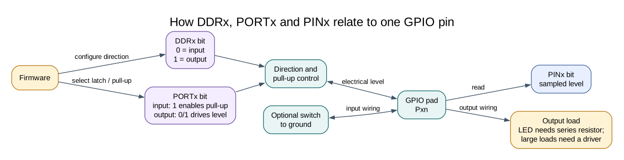
Three Registers with Different Jobs
Section titled “Three Registers with Different Jobs”Each ATmega328P I/O port uses three related registers. The x in DDRx, PORTx and PINx stands for a port letter such as B, C or D. The register names are part of the vendor device header; include <avr/io.h> rather than redefining them.
| Register | Main use | Example for Port B, bit 5 |
|---|---|---|
DDRB |
Set input (0) or output (1) direction |
`DDRB |
PORTB |
Write an output level; on an input, control its pull-up | `PORTB |
PINB |
Read sampled electrical levels on the port | if ((PINB & _BV(PINB5)) != 0U) { ... } |
On the Uno R3, D13 maps to PB5. The register-level Blink lab sets the corresponding direction bit, then changes the output latch. Port C and Port D have their own register triplets.
Set and Clear Bits Deliberately
Section titled “Set and Clear Bits Deliberately”To set one bit without changing the other bits, use a mask:
DDRB |= _BV(DDB5); /* Select PB5 as an output. */PORTB |= _BV(PORTB5); /* Drive its output latch high. */PORTB &= (uint8_t)~_BV(PORTB5); /* Drive its output latch low. */The complement is cast to the register width to make the intended 8-bit mask clear. AVR’s special register semantics matter: writing a one to a PINx bit toggles the corresponding output latch. It does not perform a normal write of a sampled input value. The HAL toggle function uses this hardware behaviour explicitly.
Read the pin with PINx; writing PORTx and reading PINx are different operations. Also give one module ownership of a port register. If an ISR and foreground code both update the same port, a read-modify-write can lose an update unless access is coordinated.
Worked Example: Read a Button
Section titled “Worked Example: Read a Button”With D2 configured as an input and its pull-up enabled, the electrical level is read from PIND bit 2. Pressing the button to ground produces a zero in that bit. The Button lab uses the HAL so the board pin mapping is explicit; the register Blink lab shows direct register access.
Exercise with Answer
Section titled “Exercise with Answer”Which register do you read to sample whether Uno D2 is low?
Answer: Read PIND and test bit 2. DDRD controls the pin direction, while PORTD controls the output latch or internal pull-up.
Code Walkthrough
Section titled “Code Walkthrough”Register-level Blink
Section titled “Register-level Blink”The example’s main() configures its peripherals, runs the algorithm and reports or displays the result. These source operations are listed in execution order:
PORTB &= (uint8_t)~_BV(PORTB5);- Sets or clears the Port B output latch. When the pin is an output, this determines its output level; on an input, it controls the pull-up.DDRB |= _BV(DDB5);- Sets the Port B direction bits; a set bit selects output mode.for (;;)- Repeats the foreground task indefinitely; each pass checks inputs, advances the calculation or services the peripheral shown below.PINB = _BV(PINB5);- Writing a one to a PINB bit toggles that pin’s PORTB output latch on the ATmega328P._delay_ms(500);- Waits for the stated interval; the foreground does no other work during this blocking delay.
Algorithm: Pin direction and output latch are separate hardware state. Expected behaviour: L toggles every 500 ms HAL source files in this repository: ATmega328P HAL on GitHub
Debounced push button
Section titled “Debounced push button”The example’s main() configures its peripherals, runs the algorithm and reports or displays the result. These source operations are listed in execution order:
avr_debounce_t button;- Use the linked public header for this function’s parameters, register ownership, blocking behavior and status values.bool level = true;- Stores this intermediate or output value for the next algorithm step. Check the units and range represented by each operand.bool led = false;- Stores this intermediate or output value for the next algorithm step. Check the units and range represented by each operand.(void)avr_gpio_mode(2U, AVR_GPIO_INPUT_PULLUP);- Maps the Uno header pin to its AVR port, sets its DDR direction bit and prepares the PORT latch for the requested initial level or pull-up.(void)avr_gpio_mode(13U, AVR_GPIO_OUTPUT);- Maps the Uno header pin to its AVR port, sets its DDR direction bit and prepares the PORT latch for the requested initial level or pull-up.avr_tick_init();- Configures the course millisecond tick interrupt source; it does not enable global interrupts itself.avr_debounce_init(&button, true, 0UL);- Seeds the stable/candidate input state and timestamp so the next transition is timed consistently.sei();- Enables global interrupts after the example has configured its sources and shared state.for (;;)- Repeats the foreground task indefinitely; each pass checks inputs, advances the calculation or services the peripheral shown below.(void)avr_gpio_read(2U, &level);- Reads the electrical level through PINx without changing direction or the output latch.if (avr_debounce_update(&button, level, avr_tick_ms(), 20U) && !button.stable)- This condition chooses the next path based on the API result. Accepts a changed input only after it remains stable for the requested interval, then reports that accepted change once.led = !led;- Stores this intermediate or output value for the next algorithm step. Check the units and range represented by each operand.(void)avr_gpio_write(13U, led);- Changes the pin’s PORT output latch; for an input pin this selects its pull-up state.
Algorithm: A candidate input must remain unchanged for 20 ms before becoming stable. No delay occurs inside an ISR. Expected behaviour: Each press toggles L once; holding the button does not repeat HAL source files in this repository: ATmega328P HAL on GitHub
include/avr_hal/gpio.hinclude/avr_hal/tick.hlib/drivers/debounce.clib/drivers/debounce.hlib/interrupts/tick.csrc/gpio.c
References
Section titled “References”- Microchip, ATmega328P product documentation, I/O ports and register descriptions.
- Uno pin names and alternate functions
- GPIO concepts