PCD8544 Nokia 5110 Display
Learning Goals
Section titled “Learning Goals”This lesson uses the Uno hardware SPI peripheral to write to a PCD8544 display. You will see how the controller divides its display RAM into pages and why a full framebuffer is a poor fit for a small SRAM device.
The Display Memory Layout
Section titled “The Display Memory Layout”The PCD8544 drives 84 columns by 48 rows of monochrome pixels. A full image needs one bit for each pixel:
84 columns × 48 rows ÷ 8 bits per byte = 504 bytesThe Uno has only 2 KB of SRAM for global variables, local variables and the stack. Reserving 504 bytes for a screen can leave little room for the rest of a program. The driver in this lesson writes one 8-row page at a time, using an 84-byte buffer.
The display RAM has six pages. Each byte represents one column of eight vertical pixels; the page index selects which group of eight rows is updated. The example clears the display, then writes a simple alternating pattern to page 2.
Check Supply and Logic Levels
Section titled “Check Supply and Logic Levels”The PCD8544 controller IC is a low-voltage device. Many hobby modules include extra components, but layouts and input protection differ. Check your exact board’s supply range and logic levels before connecting it to the 5 V Uno. If the display inputs are not 5 V tolerant, use suitable level translation for CS, D/C, RESET, DIN and CLK. No display MISO connection is used.
| Arduino Uno R3 | Display Module | Note |
|---|---|---|
| D7 | CS | Active-low chip select |
| D8 | D/C | LOW sends commands; HIGH sends display data |
| D9 | RESET | Active-low hardware reset |
| D11 / COPI | DIN | SPI controller output |
| D13 / SCK | CLK | SPI clock |
| GND | GND | Common ground |
| Supply | VCC or VIN as specified by the breakout maker | Do not assume every Nokia 5110 board accepts 5 V |
The SPI HAL also configures D10 as an output and uses D10–D13 for the SPI peripheral. The PCD8544 driver therefore rejects D10–D13 for its separate control pins.
Commands and Pixel Data
Section titled “Commands and Pixel Data”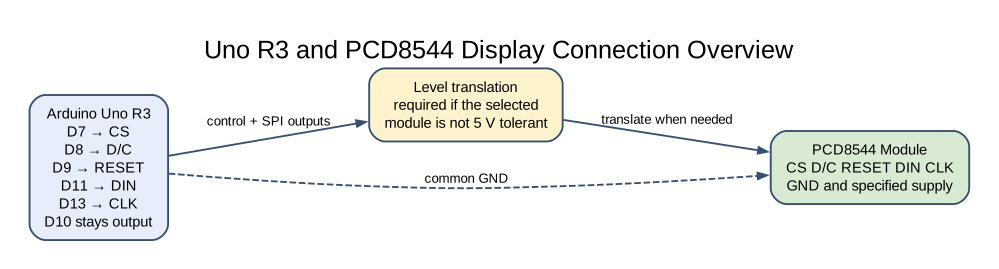
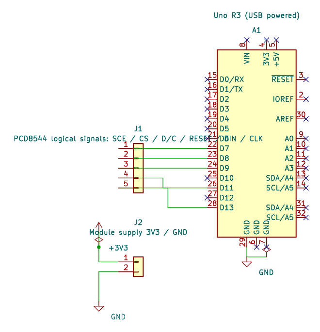
The editable KiCad pin map records the Uno-side signal assignments. Check the actual breakout pinout and add translation on any 5 V output that reaches a 3.3 V-only input.
The driver selects SPI mode 0 at 2 MHz. It resets the module, enters extended instruction mode, sets the requested contrast and bias, returns to basic mode and selects normal display operation. The contrast value is a starting point; the panel’s ideal setting depends on its LCD glass and module design.
To write one page, the driver sets the column and page addresses, switches D/C to data mode and sends 84 bytes. Each SPI wait is bounded by the shared HAL poll budget. On failure, the driver deasserts CS and returns the error. A partial write may have advanced the controller address, so reinitialize before retrying.
Build and Observe
Section titled “Build and Observe”Build the experiment with both available toolchains:
python atmega328p-labs/tools/build.py 52-pcd8544 --compiler gccpython atmega328p-labs/tools/build.py 52-pcd8544 --compiler xc8Upload the generated HEX through the Uno bootloader after checking your module’s voltage requirements. The display should show alternating black and white vertical blocks in one 8-pixel-high band; the other five pages should remain blank. Adjust the contrast setting in main.c a little at a time if the pixels are difficult to see.
Source Files
Section titled “Source Files”- PCD8544 Public Driver Header
- PCD8544 Driver Implementation
- Uno Page-Buffer Example
- Wiring And Exercise Metadata
- SPI Fundamentals
Troubleshooting
Section titled “Troubleshooting”- Blank screen: check the breakout power, ground, RESET level, CS and SPI wiring before changing contrast.
- Random pixels: confirm D/C is LOW for commands and HIGH for page bytes, and verify the module’s SPI clock timing.
- Very dark or faint pixels: adjust contrast within the controller’s documented range; the correct value varies by LCD panel.
- Display works with a different board but not the Uno: check 5 V signal levels, pin mapping and SPI clock frequency.
- Unexpected output on D13: D13 is also the Uno’s SPI clock pin and its onboard LED may flicker during transfers.
Code Walkthrough
Section titled “Code Walkthrough”PCD8544 Page Buffer Display
Section titled “PCD8544 Page Buffer Display”The example’s main() configures its peripherals, runs the algorithm and reports or displays the result. These source operations are listed in execution order:
avr_pcd8544_t display;- Use the linked public header for this function’s parameters, register ownership, blocking behavior and status values.if (avr_pcd8544_init(&display, 7U, 8U, 9U, 50U) != AVR_OK)- This checks for any setup or transfer error before the program continues. Use the linked public header for this function’s parameters, register ownership, blocking behavior and status values.return 1;- Stops this path and returns the indicated status when setup or validation cannot continue.for (uint8_t page = 0U; page < AVR_PCD8544_PAGES; page++)- Repeats whilepage < AVR_PCD8544_PAGESis true;uint8_t page = 0Usets the starting state andpage++advances it each pass.for (uint8_t column = 0U; column < AVR_PCD8544_COLUMNS; column++)- Repeats whilecolumn < AVR_PCD8544_COLUMNSis true;uint8_t column = 0Usets the starting state andcolumn++advances it each pass.page_data[column] = ((page == 2U) && (((column / 6U) % 2U) == 0U)) ? UINT8_MAX : 0U;- Stores this intermediate or output value for the next algorithm step. Check the units and range represented by each operand.if (avr_pcd8544_write_page(&display, page, page_data) != AVR_OK)- This checks for any setup or transfer error before the program continues. Use the linked public header for this function’s parameters, register ownership, blocking behavior and status values.for (;;)- Repeats the foreground task indefinitely; each pass checks inputs, advances the calculation or services the peripheral shown below._delay_ms(1000);- Waits for the stated interval; the foreground does no other work during this blocking delay.
Algorithm: The driver writes the display’s six 84-byte pages one at a time using a single 84-byte application buffer instead of a 504-byte framebuffer. Expected behaviour: One 8-pixel-high band shows alternating 6-column blocks; the remaining display pages are blank HAL source files in this repository: ATmega328P HAL on GitHub
Check Your Understanding
Section titled “Check Your Understanding”- How many bytes does a full 84 by 48 monochrome image need?
- How much SRAM does the example allocate for a page of pixel data?
- Why does the driver deassert CS after an SPI error?
Suggested answers: A full frame needs 504 bytes. One page uses 84 bytes. CS is deasserted so the peripheral is not left selected after an incomplete transaction; the controller may still need reinitialization before retrying.
References
Section titled “References”- Philips Semiconductors, PCD8544 Product Specification, 12 April 1999. The document specifies the 84-column by 48-row display RAM, serial interface timing and low-voltage supply.
- Microchip, ATmega328P Device Documentation, SPI chapter and Uno pin mapping.
- See the Arduino Uno R3 Pinout for board header locations.
Validation status: AVR GCC and XC8 builds are required for the example. No physical module is available here; wiring, contrast and visible output remain unverified.